Semiconductor device and method of controlling said semiconductor device
a semiconductor device and semiconductor technology, applied in the direction of static storage, digital storage, instruments, etc., can solve the problems of inaccurate reading, circuit size cannot be reduced, and leakage current caused in unselected blocks at the time of reading or programming has become a problem, so as to reduce circuit size, accurate reading, and the effect of restricting leakage in unselected blocks
- Summary
- Abstract
- Description
- Claims
- Application Information
AI Technical Summary
Benefits of technology
Problems solved by technology
Method used
Image
Examples
first embodiment
(First Embodiment)
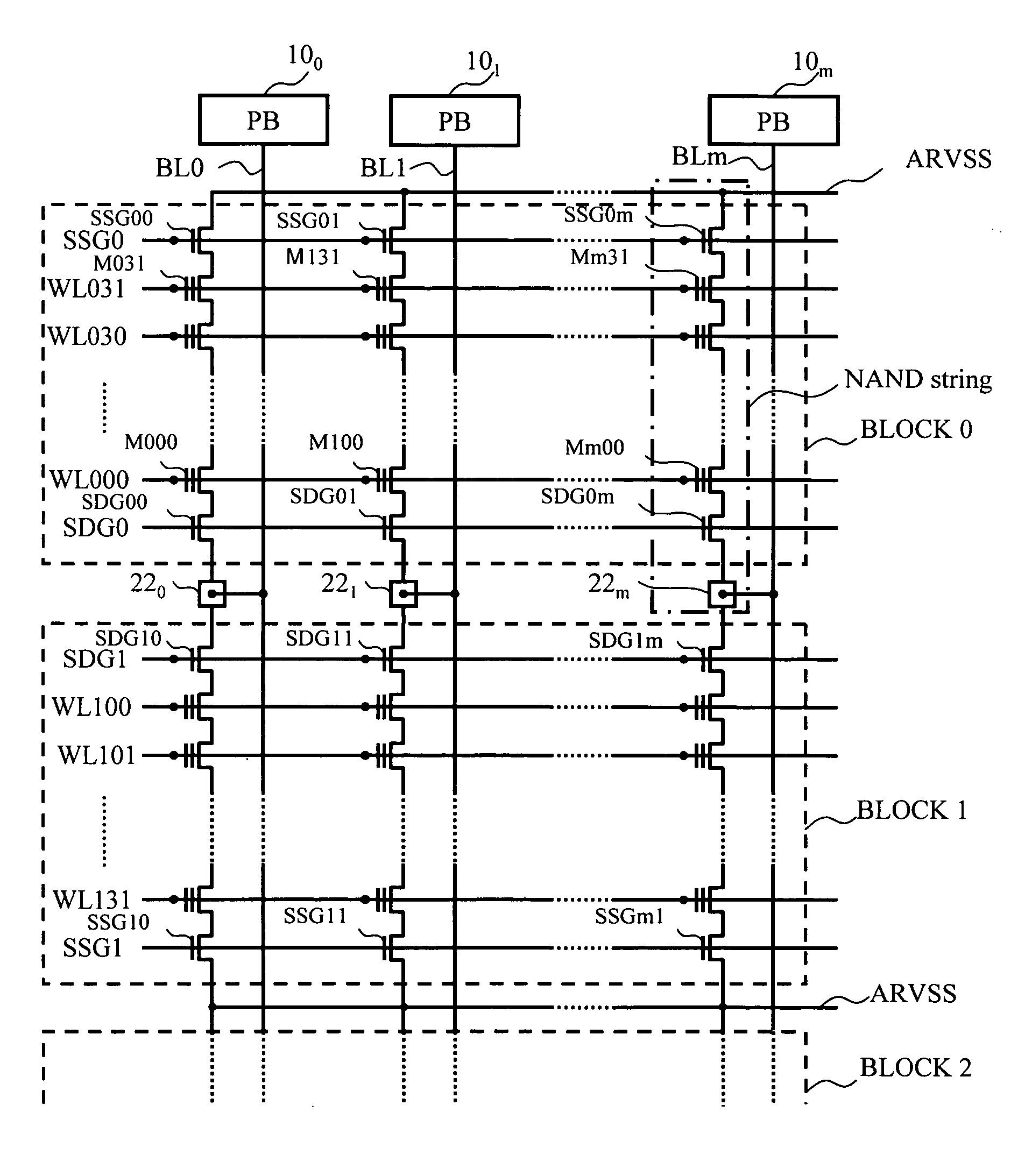
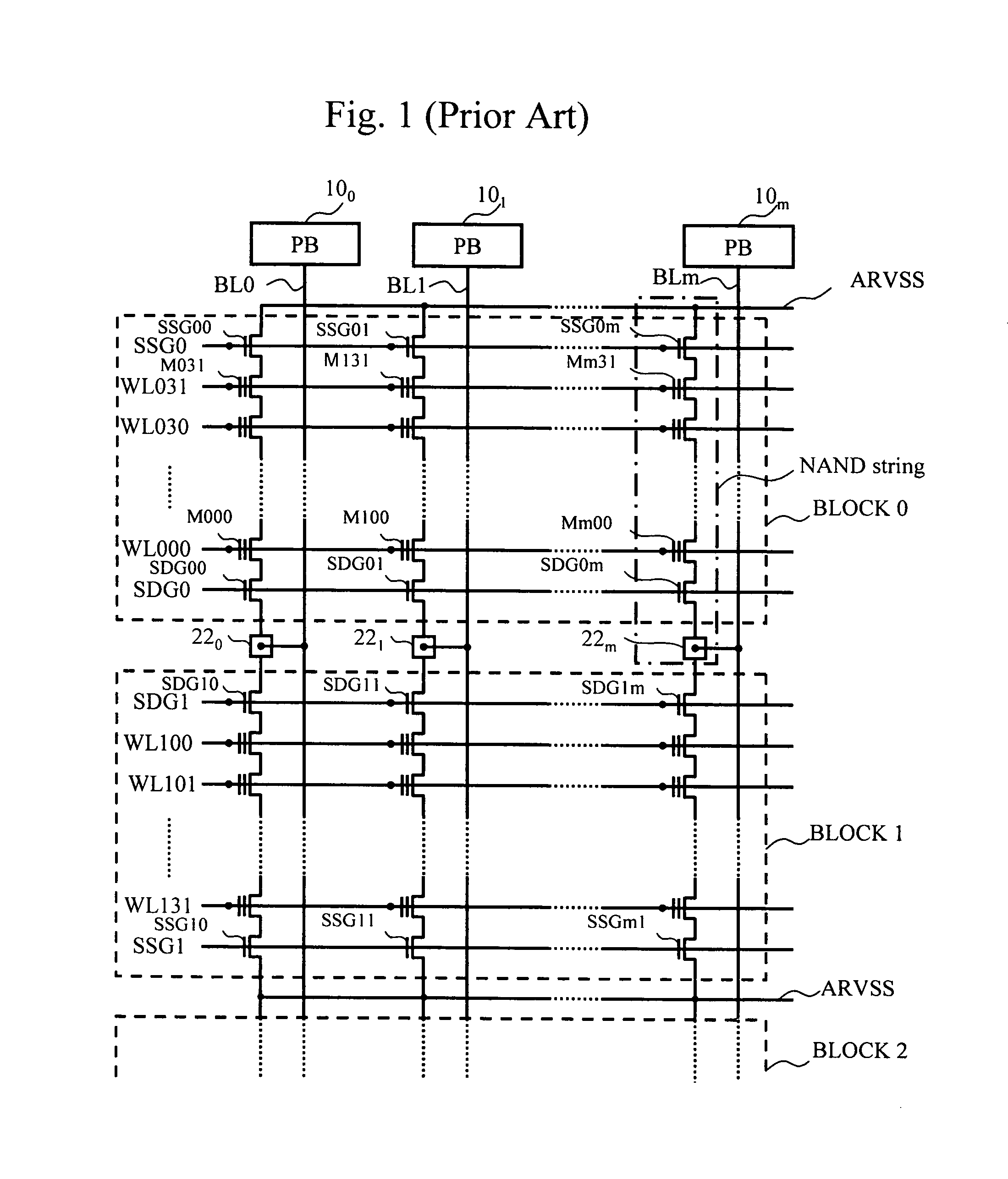
[0050]FIG. 5 is a block diagram of a NAND flash memory in accordance with a first embodiment of the present invention. The flash memory 51 includes a memory cell array 52, an I / O register buffer 53, an address register 54, a status register 55, a command register 56, a state machine 57, a high-voltage generating circuit 58, a row decoder 59, a page buffer 60, and a column decoder 61.
[0051]The memory cell array 52 has rewritable non-volatile memory cell transistors aligned with word lines WL and bit lines BL that are arranged in a matrix fashion.
[0052]The I / O register buffer 53 controls various signals and data corresponding to I / O terminals. The address register 54 temporarily stores address signals that are input through the I / O register buffer 53. The status register 55 temporarily stores status information. The command register 56 temporarily stores operation commands that are input through the I / O register buffer 53.
[0053]The state machine 57 controls the opera...
second embodiment
(Second Embodiment)
[0065]Next, a second embodiment of the present invention is described. FIG. 9 illustrates a FG-type NAND flash memory array and sense voltage conditions for reading in accordance with the second embodiment. Table 2 shows the conditions for reading in a selected block and an unselected block in the second embodiment.
[0066]
TABLE 2UNSELECTEDBLOCKSELECTED BLOCK (BLOCK 0)(BLOCK 1)Sel WLUnsel WLSDGSSGWLSDGSSGARVSSBLPre-chargeVpass(4 V)Vpass(4 V)Vpass(4 V)0 VFloating0 V0 V0 V1 VSenseVread(0 V)Vpass (4 V)Vpass (4 V)VccFloating0 V0 V0 Vsensed
[0067]In FIG. 9, reference numeral 152 indicates a memory cell array, and reference numeral 60m indicates a page buffer. Thirty-two FG-type memory cells are connected in series, so as to form a NAND string. A select drain gate SDG0m and a select source gate SSG0m are connected to both ends of each NAND string. In FIG. 9, the block BLOCK0 is a selected block, and the block BLOCK1 is an unselected block.
[0068]The second embodiment is cha...
third embodiment
(Third Embodiment)
[0076]Next, a third embodiment of the present invention is described. FIG. 13 illustrates the array structure of a SONOS-type NAND flash memory in accordance with the third embodiment. In FIG. 13, reference numeral 252 indicates the memory cell array, and 60m indicates a page buffer. Sixteen SONOS-type memory cells are connected in series, so as to form a NAND string. A select drain gate SDG0m and a select source gate SSG0m are connected to both ends of each NAND string. The select drain gates SDG are also of a SONOS type. The select drain gate SDG0m is further connected to the bit line BLm via a drain contact 22m, and the bit line BLm is connected to the page buffer 60m. The block formed with m (m being 512 bytes+16 bytes) of NAND strings forms one erasing unit.
[0077]The m of memory cells that are connected to one word line WL form one page that is an access unit for reading and programming. Accordingly, reading and programming can be performed simultaneously on t...
PUM
 Abstract
Description
Claims
Application Information
 - R&D
- Intellectual Property
- Life Sciences
- Materials
- Tech Scout
- Unparalleled Data Quality
- Higher Quality Content
- 60% Fewer Hallucinations
Browse by: Latest US Patents, China's latest patents, Technical Efficacy Thesaurus, Application Domain, Technology Topic, Popular Technical Reports.
© 2025 PatSnap. All rights reserved.Legal|Privacy policy|Modern Slavery Act Transparency Statement|Sitemap|About US| Contact US: help@patsnap.com


