
Method and apparatus for drying semiconductor wafer surfaces using a plurality of inlets and outlets held in close proximity to the wafer surfaces

Inactive Publication Date: 2007-06-26
LAM RES CORP
View PDF92 Cites 58 Cited by
  • Summary
  • Abstract
  • Description
  • Claims
  • Application Information

AI Technical Summary

Benefits of technology

[0010]Broadly speaking, the present invention fills these needs by providing a cleaning and drying apparatus that is capable of removing fluids from wafer surfaces quickly while at the same time reducing wafer contamination. It should be appreciated that the present invention can be implemented in numerous ways, including as a process, an apparatus, a system, a device or a method. Several inventive embodiments of the present invention are described below.
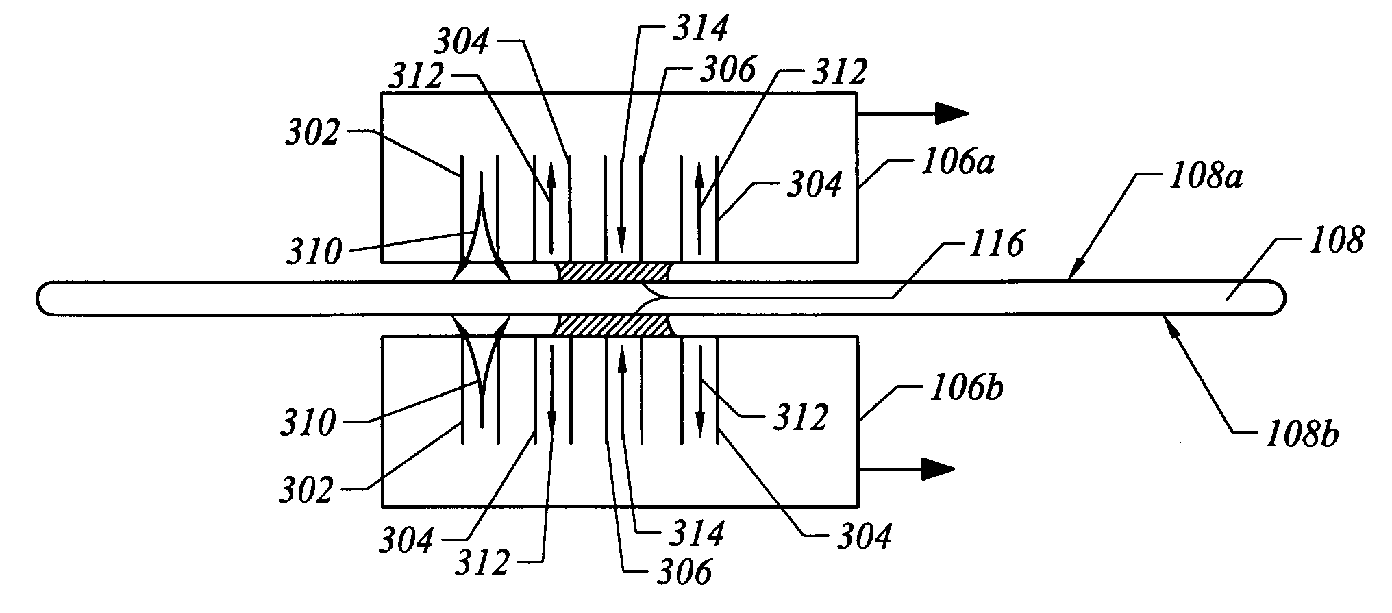
[0017]The advantages of the present invention are numerous. Most notably, the apparatuses and methods described herein efficiently dry and clean a semiconductor wafer while reducing fluids and contaminants remaining on a wafer surface. Consequently, wafer processing and production may be increased and higher wafer yields may be achieved due to efficient wafer drying with lower levels of contamination. The present invention enables the improved drying and cleaning through the use of vacuum fluid removal in conjunction with fluid input. The pressures generated on a fluid film at the wafer surface by the aforementioned forces enable optimal removal of fluid at the wafer surface with a significant reduction in remaining contamination as compared with other cleaning and drying techniques. In addition, the present invention may utilize application of an isopropyl alcohol (IPA) vapor and deionized water towards a wafer surface along with generation of a vacuum near the wafer surface at substantially the same time. This enables both the generation and intelligent control of a meniscus and the reduction of water surface tension along a deionized water interface and therefore enables optimal removal of fluids from the wafer surface without leaving contaminants. The meniscus generated by input of IPA, DIW and output of fluids may be moved along the surface of the wafer to clean and dry the wafer. Therefore, the present invention evacuates fluid from wafer surfaces with extreme effectiveness while substantially reducing contaminant formation due to ineffective drying such as for example, spin drying.

Problems solved by technology

Unfortunately, this process tends to leave an accumulation of slurry particles and residues at the wafer surface.
If left on the wafer, the unwanted residual material and particles may cause, among other things, defects such as scratches on the wafer surface and inappropriate interactions between metallization features.
In some cases, such defects may cause devices on the wafer to become inoperable.
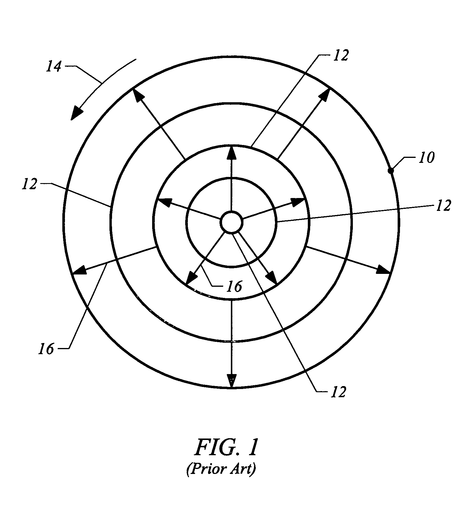
Unfortunately, if the moving liquid / gas interface breaks down, as often happens with all of the aforementioned drying methods, droplets form and evaporation occurs resulting in contaminants being left on the wafer surface.
As stated previously, if the moving liquid / gas interface 12 breaks down, droplets of the cleaning fluid form on the wafer and contamination may occur due to evaporation of the droplets.
Unfortunately, the present drying methods are only partially successful at the prevention of moving liquid interface breakdown.
In addition, the SRD process has difficulties with drying wafer surfaces that are hydrophobic.
Hydrophobic wafer surfaces can be difficult to dry because such surfaces repel water and water based (aqueous) cleaning solutions.
Therefore, because of the hydrophobic interactions and the surface tension, balls (or droplets) of aqueous cleaning fluid forms in an uncontrolled manner on the hydrophobic wafer surface.
This formation of droplets results in the harmful evaporation and the contamination discussed previously.
The limitations of the SRD are particularly severe at the center of the wafer, where centrifugal force acting on the droplets is the smallest.
Consequently, although the SRD process is presently the most common way of wafer drying, this method can have difficulties reducing formation of cleaning fluid droplets on the wafer surface especially when used on hydrophobic wafer surfaces.
Such deposits as often occurs today reduce the yield of acceptable wafers and increase the cost of manufacturing semiconductor wafers.

Method used


Image

  • Method and apparatus for drying semiconductor wafer surfaces using a plurality of inlets and outlets held in close proximity to the wafer surfaces
  • Method and apparatus for drying semiconductor wafer surfaces using a plurality of inlets and outlets held in close proximity to the wafer surfaces
  • Method and apparatus for drying semiconductor wafer surfaces using a plurality of inlets and outlets held in close proximity to the wafer surfaces

Examples


Embodiment Construction

[0067]An invention for methods and apparatuses for cleaning and / or drying a wafer is disclosed. In the following description, numerous specific details are set forth in order to provide a thorough understanding of the present invention. It will be understood, however, by one of ordinary skill in the art, that the present invention may be practiced without some or all of these specific details. In other instances, well known process operations have not been described in detail in order not to unnecessarily obscure the present invention.

[0068]While this invention has been described in terms of several preferred embodiments, it will be appreciated that those skilled in the art upon reading the preceding specifications and studying the drawings will realize various alterations, additions, permutations and equivalents thereof. It is therefore intended that the present invention includes all such alterations, additions, permutations, and equivalents as fall within the true spirit and scop...


PUM


Abstract

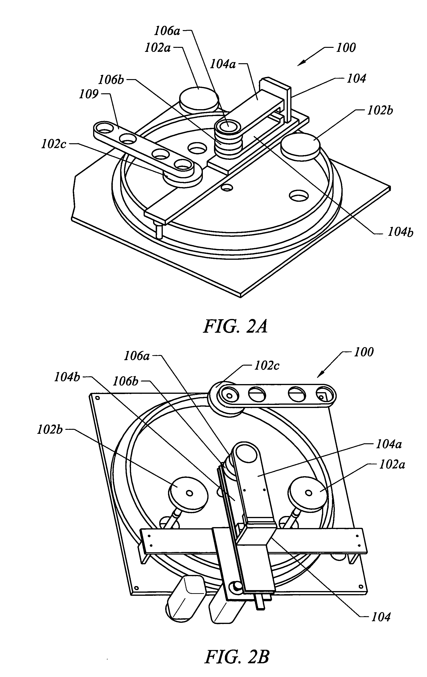
One of many embodiments of a substrate preparation system is provided which includes a head having a head surface where the head surface is proximate to a surface of the substrate. The system also includes a first conduit for delivering a first fluid to the surface of the substrate through the head, and a second conduit for delivering a second fluid to the surface of the substrate through the head, where the second fluid is different than the first fluid. The system also includes a third conduit for removing each of the first fluid and the second fluid from the surface of the substrate where the first conduit, the second conduit and the third conduit act substantially simultaneously.

Description

CROSS REFERENCE TO RELATED APPLICATION[0001]This is a continuation-in-part of U.S. patent application Ser. No. 09 / 608,244 entitled “Capillary Proximity Heads for Single Wafer Cleaning and Drying” filed on Jun. 30, 2000 now U.S. Pat. No. 6,488,040. The aforementioned patent application is hereby incorporated by reference.BACKGROUND OF THE INVENTION[0002]1. Field of the Invention[0003]The present invention relates to semiconductor wafer cleaning and drying and, more particularly, to apparatuses and techniques for more efficiently removing fluids from wafer surfaces while reducing contamination and decreasing wafer cleaning cost.[0004]2. Description of the Related Art[0005]In the semiconductor chip fabrication process, it is well-known that there is a need to clean and dry a wafer where a fabrication operation has been performed that leaves unwanted residues on the surfaces of wafers. Examples of such a fabrication operation include plasma etching (e.g., tungsten etch back (WEB)) and c...

Claims


Application Information

Patent Timeline
IPC IPC(8): B08B3/00F26B5/04B08B3/04H01L21/00
CPCB08B3/04G03F7/30H01L21/67028H01L21/67034H01L21/67051Y10S134/902
Inventor DE LARIOS, JOHN M.RAVKIN, MIKEWOODS, CARLREDEKER, FRITZGARCIA, JAMES P.NICKHOU, AFSHIN
Owner LAM RES CORP
Learn More