Supercharge Your Innovation With Domain-Expert AI Agents!

CMOS image sensor with voltage control circuit

Inactive Publication Date: 2007-05-29
SOCIONEXT INC
View PDF8 Cites 34 Cited by
  • Summary
  • Abstract
  • Description
  • Claims
  • Application Information

AI Technical Summary

Benefits of technology

[0020]The present invention was made under the background circumstances as described above. An object of the present invention is to provide a CMOS image sensor which can reduce wideband kTC noise.

Problems solved by technology

However, these CCDs have the drawbacks of the need for a plurality of power supply circuits, a high driving voltage, and high power consumption.
Therefore, attention has recently been riveted to CMOS image sensors that can be produced by the process for producing complementary metal-oxide semiconductors (CMOSes), which can operate at a low voltage, which consume only a small amount of power, and the unit cost of the production of which is low.
This kTC noise is produced at random, so it is comparatively difficult to remove the kTC noise from image signals.
There are many cases where high-frequency kTC noise cannot be removed.
This method can reduce kTC noise components in a frequency band where this differential amplifier operates, but it cannot reduce kTC noise components at frequencies higher than that frequency band.
Moreover, there are many cases where a circuit for reducing kTC noise is comparatively large-scale.

Method used


Image

  • CMOS image sensor with voltage control circuit
  • CMOS image sensor with voltage control circuit
  • CMOS image sensor with voltage control circuit

Examples


Embodiment Construction

[0032]Embodiments of the present invention will now be described with reference to the drawings.

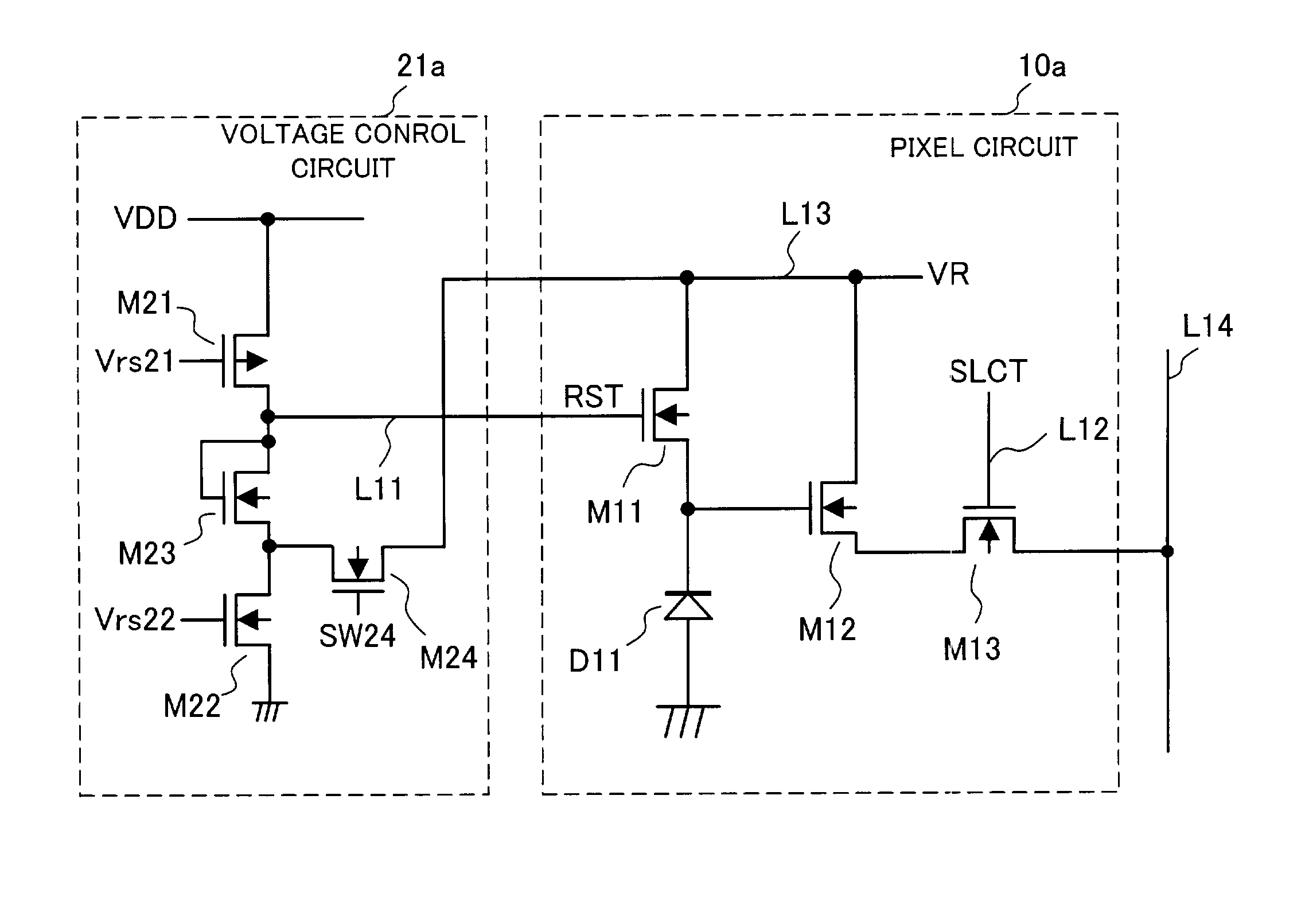
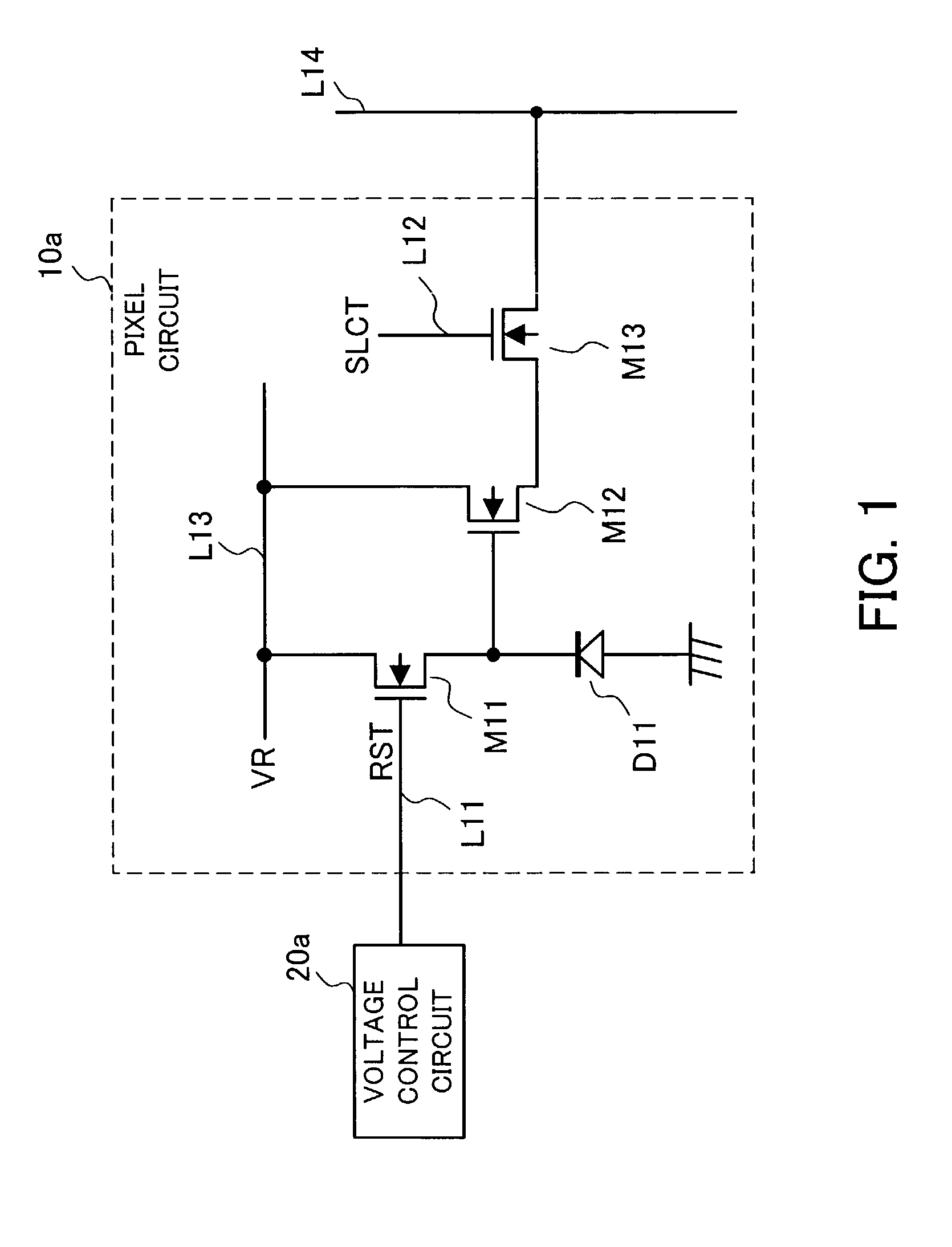
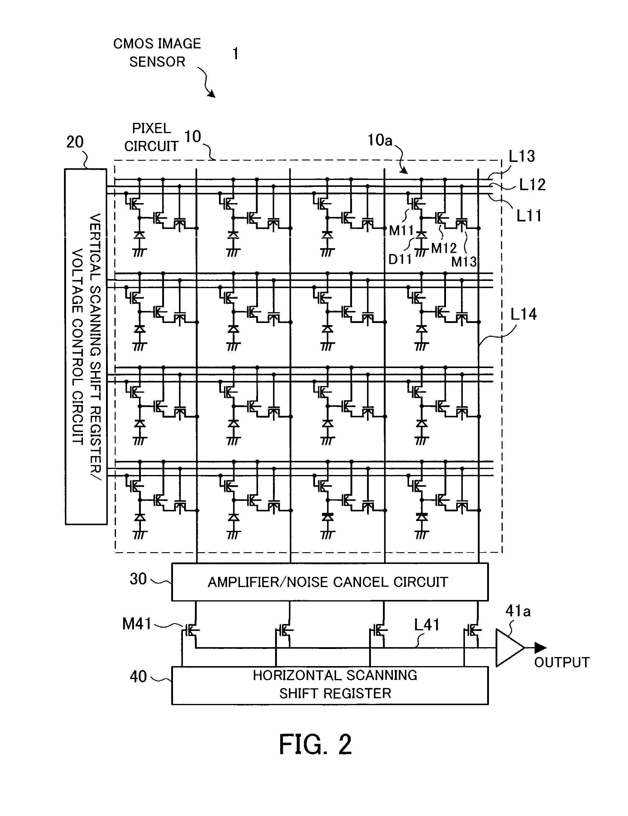
[0033]FIG. 2 is a view showing the entire structure of a CMOS image sensor according to the present invention.

[0034]As shown in FIG. 2, a CMOS image sensor 1 according to the present invention comprises a pixel section 10 where pixel circuits 10a are arranged like a matrix, a vertical scanning shift register / voltage control circuit 20 for specifying the pixel circuits 10a in a vertical direction and for controlling the voltage of a reset signal, an amplifier / noise cancel circuit 30 for performing the processes of amplifying image signals output from the pixel circuits 10a in each column and reducing noise included in them, and a horizontal scanning shift register 40 for specifying output from the pixel circuits 10a in a horizontal direction by column selection transistors M41. Moreover, an amplifier 41a is connected to an output bus L41 which accepts a signal output from each column selec...


PUM


Abstract

A CMOS image sensor that reduces kTC noise in a wide band. A pixel circuit corresponding to one pixel includes a photoelectric conversion element for carrying out the photoelectric conversion of incident light, a reset transistor for resetting a cathode of the photoelectric conversion element to initial voltage, an amplifying transistor for converting electric charges accumulated in the photoelectric conversion element to voltage, and a row selection transistor for selecting signals output from pixel areas arranged in a row direction. A voltage control circuit controls the potential of a gate of the reset transistor during a period when the photoelectric conversion element is reset to change ON-state resistance of the reset transistor. By doing so, a cutoff frequency for a low-pass filter formed in the pixel circuit by ON-state resistance of the reset transistor and parasitic capacitance produced at the cathode on the photoelectric conversion element will be controlled.

Description

CROSS-REFERENCE TO RELATED APPLICATIONS[0001]This application is based upon and claims priority of Japanese Patent Application No. 2002-29633, filed on Feb. 6, 2002, the contents being incorporated herein by reference.BACKGROUND OF THE INVENTION[0002](1) Field of the Invention[0003]This invention relates to a CMOS image sensor for getting images by outputting in order image signals sensed in each of pixel areas arranged like a matrix on the basis of X-Y addressing and, more particularly, to a CMOS image sensor which can reduce kTC noise.[0004](2) Description of the Related Art[0005]With the spread of digital still-image cameras and digital video cameras, the addition of a camera function to cellular telephones, and the like, a demand for solid imaging devices has risen in recent years. At present charge coupled devices (CCDs) have spread most widely as solid imaging devices. However, these CCDs have the drawbacks of the need for a plurality of power supply circuits, a high driving v...

Claims


Application Information

Patent Timeline
IPC IPC(8): H04N3/14H04N5/335H01L27/146H04N5/357H04N5/359H04N5/363H04N5/369H04N5/374H04N5/3745
CPCH04N5/363H04N5/3575H04N25/616H04N25/65H04N25/77
Inventor KOKUBUN, MASATOSHITSUCHIYA, CHIKARA
Owner SOCIONEXT INC
Features
  • R&D
  • Intellectual Property
  • Life Sciences
  • Materials
  • Tech Scout
  • Unparalleled Data Quality
  • Higher Quality Content
  • 60% Fewer Hallucinations
Learn More