Miniature surface plasmon resonance waveguide device with sinusoidal curvature compensation
a technology of surface plasmon resonance and sensing device, which is applied in the direction of optical waveguide light guide, optical element, instrument, etc., can solve the problems of waveguide design, lack of optimal size, and inability to offer a handy user interfa
- Summary
- Abstract
- Description
- Claims
- Application Information
AI Technical Summary
Benefits of technology
Problems solved by technology
Method used
Image
Examples
first embodiment
The First Embodiment
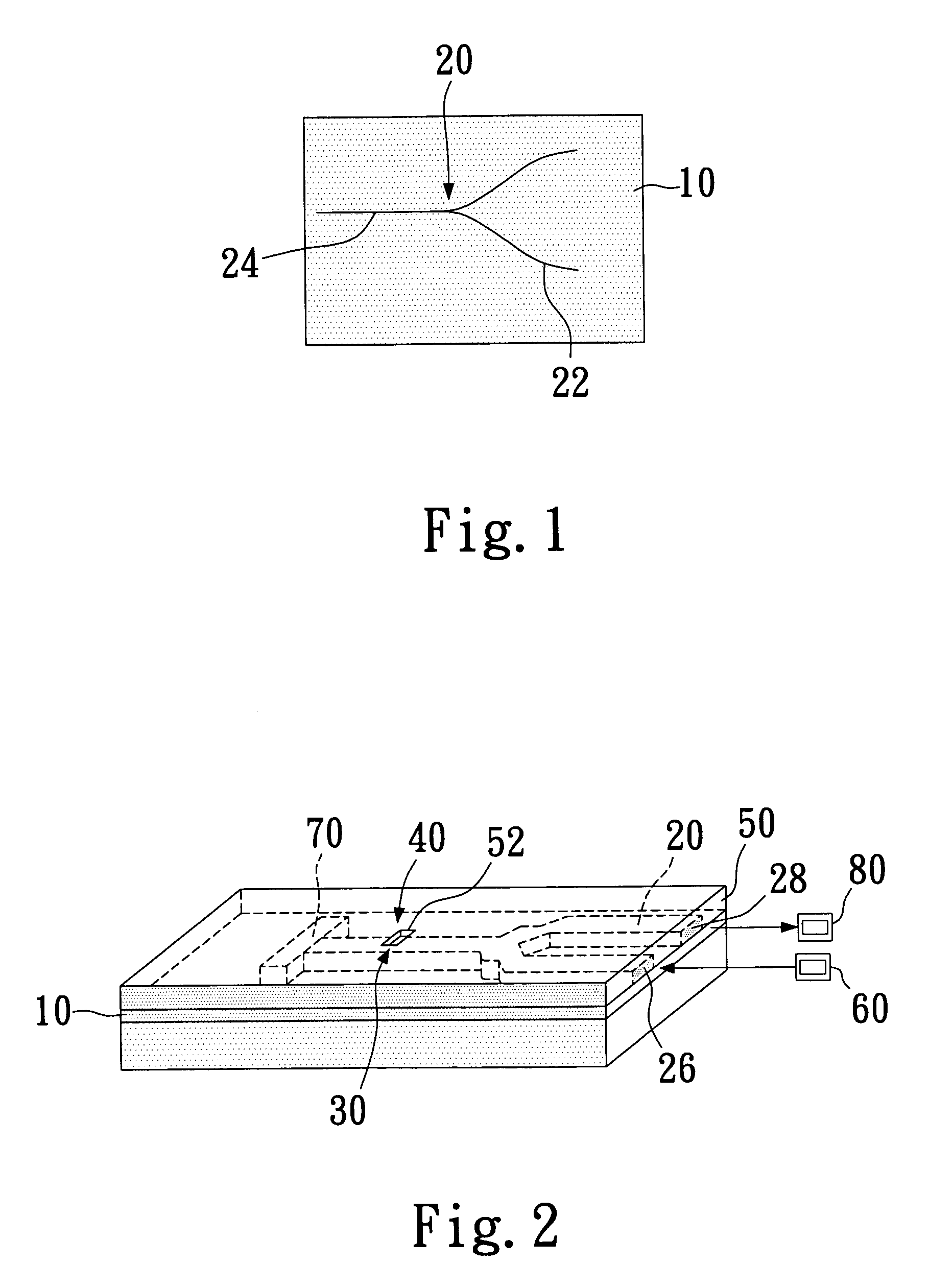
[0069]FIG. 1 is a schematic view of a miniature SPR waveguide device with dual sinusoidal curvatures for compensation of the present invention. An waveguide structure 20 on a substrate 10 has dual sinusoidal curvatures 22 for compensation which combine to form a Y-shaped structure 24.
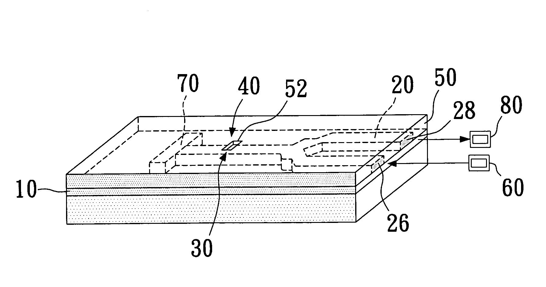
[0070]FIG. 2 is a sectional side view of a miniature SPR waveguide device with dual sinusoidal curvatures for compensation of the present invention. The miniature SPR waveguide device 100 with dual sinusoidal curvatures for compensation comprises: a substrate 10; an waveguide structure 20, having sinusoidal curvatures for compensation and resting on top of the substrate 10; a sensing film layer 30, standing at a specific area on top of the waveguide structure 20 where the specific area is a sensing area 40; and a cover layer 50, covering the whole device and having a hole 52 around the sensing area 40; wherein the waveguide structure 20 possesses a light beam input port 26 and a ligh...
second embodiment
The Second Embodiment
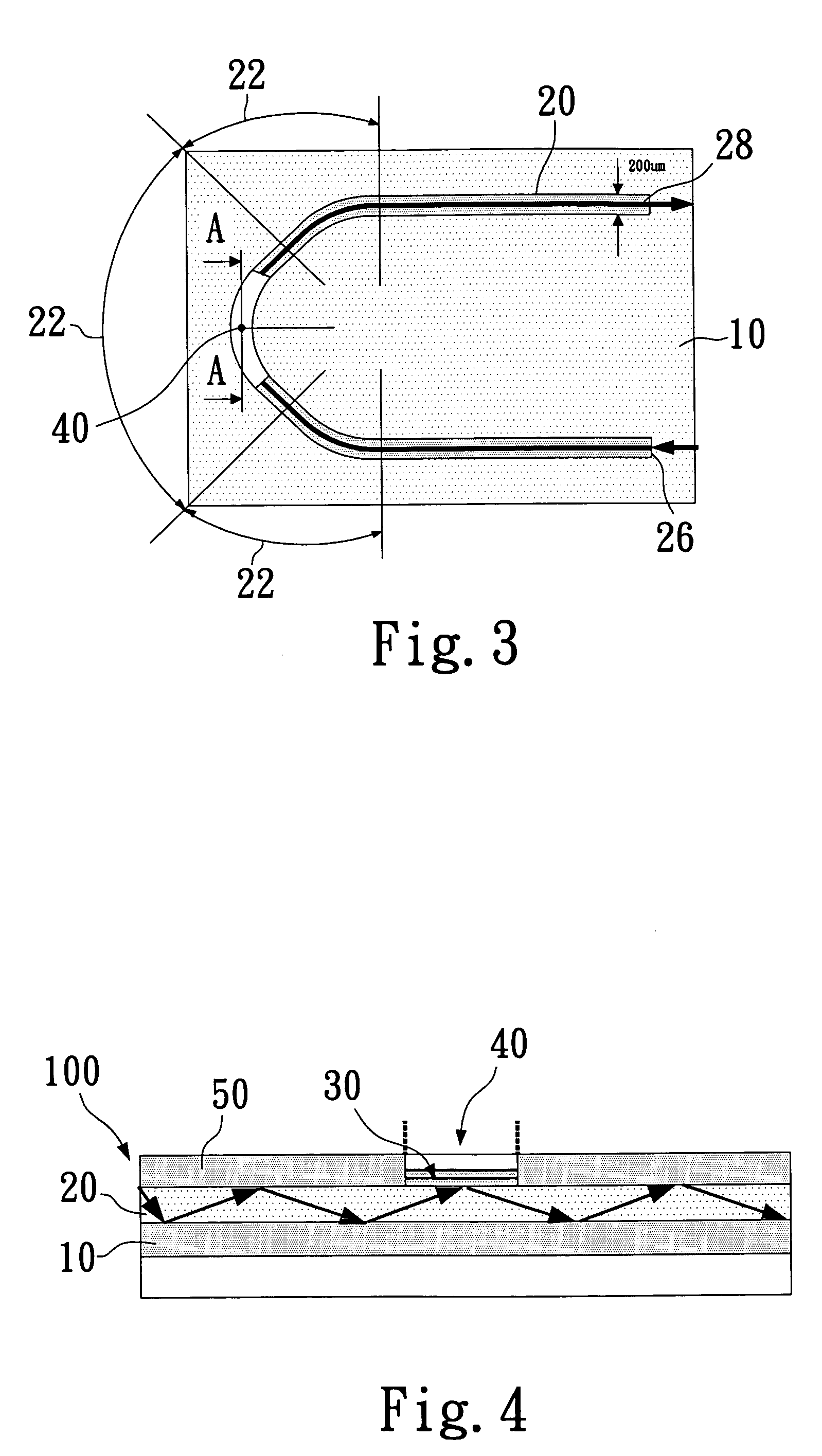
[0072]FIG. 3 is a schematic view of another embodiment of the present invention. An waveguide structure 20 on top of a substrate 10 has a shape with triple sinusoidal curvatures 22 for compensation.
[0073]FIG. 4 is a sectional side view showing the portion of A–A′ of FIG. 3. A miniature SPR waveguide device 100 with dual sinusoidal curvatures for compensation comprises: a substrate 10; an waveguide structure 20, having dual sinusoidal curvatures for compensation and resting on top of the substrate 10; a sensing film layer 30, standing at a specific area on top of the waveguide structure 20 where the specific area is a sensing area 40; and a cover layer 50, covering the whole device and having a hole 52 around the sensing area 40; wherein the waveguide structure 20 possesses a light beam input port 26 and a light beam output port 28.
[0074]In this embodiment, the sensing film 30 is made by a gold (Au) film and a silver (Ag) film, and the Au film is deposited on top...
PUM
| Property | Measurement | Unit |
|---|---|---|
| guide wavelengths | aaaaa | aaaaa |
| guide wavelengths | aaaaa | aaaaa |
| width | aaaaa | aaaaa |
Abstract
Description
Claims
Application Information
 - R&D
- Intellectual Property
- Life Sciences
- Materials
- Tech Scout
- Unparalleled Data Quality
- Higher Quality Content
- 60% Fewer Hallucinations
Browse by: Latest US Patents, China's latest patents, Technical Efficacy Thesaurus, Application Domain, Technology Topic, Popular Technical Reports.
© 2025 PatSnap. All rights reserved.Legal|Privacy policy|Modern Slavery Act Transparency Statement|Sitemap|About US| Contact US: help@patsnap.com


