Semiconductor integrated circuit and method of testing semiconductor integrated circuit

a technology of integrated circuits and semiconductors, applied in the field of testing roms, can solve the problems of increasing man-hours and mask design costs, and achieve the effect of sufficient level of security

Inactive Publication Date: 2007-02-27
PANASONIC SEMICON SOLUTIONS CO LTD
View PDF14 Cites 4 Cited by
  • Summary
  • Abstract
  • Description
  • Claims
  • Application Information

AI Technical Summary

Benefits of technology

[0006]It is therefore an object of the present invention to make a ROM directly testable externally while ensuring a sufficient level of security for the confidential information stored on the ROM.

Problems solved by technology

However, to modify the contents of the confidential information, the BIST circuit itself, built in a semiconductor circuit, should be redesigned, thus considerably increasing the man-hour, the mask design cost and so on needed for the redesign process.

Method used


Image

  • Semiconductor integrated circuit and method of testing semiconductor integrated circuit
  • Semiconductor integrated circuit and method of testing semiconductor integrated circuit
  • Semiconductor integrated circuit and method of testing semiconductor integrated circuit

Examples


Embodiment Construction

[0017]Hereinafter, preferred embodiments of the present invention will be described with reference to the accompanying drawings.

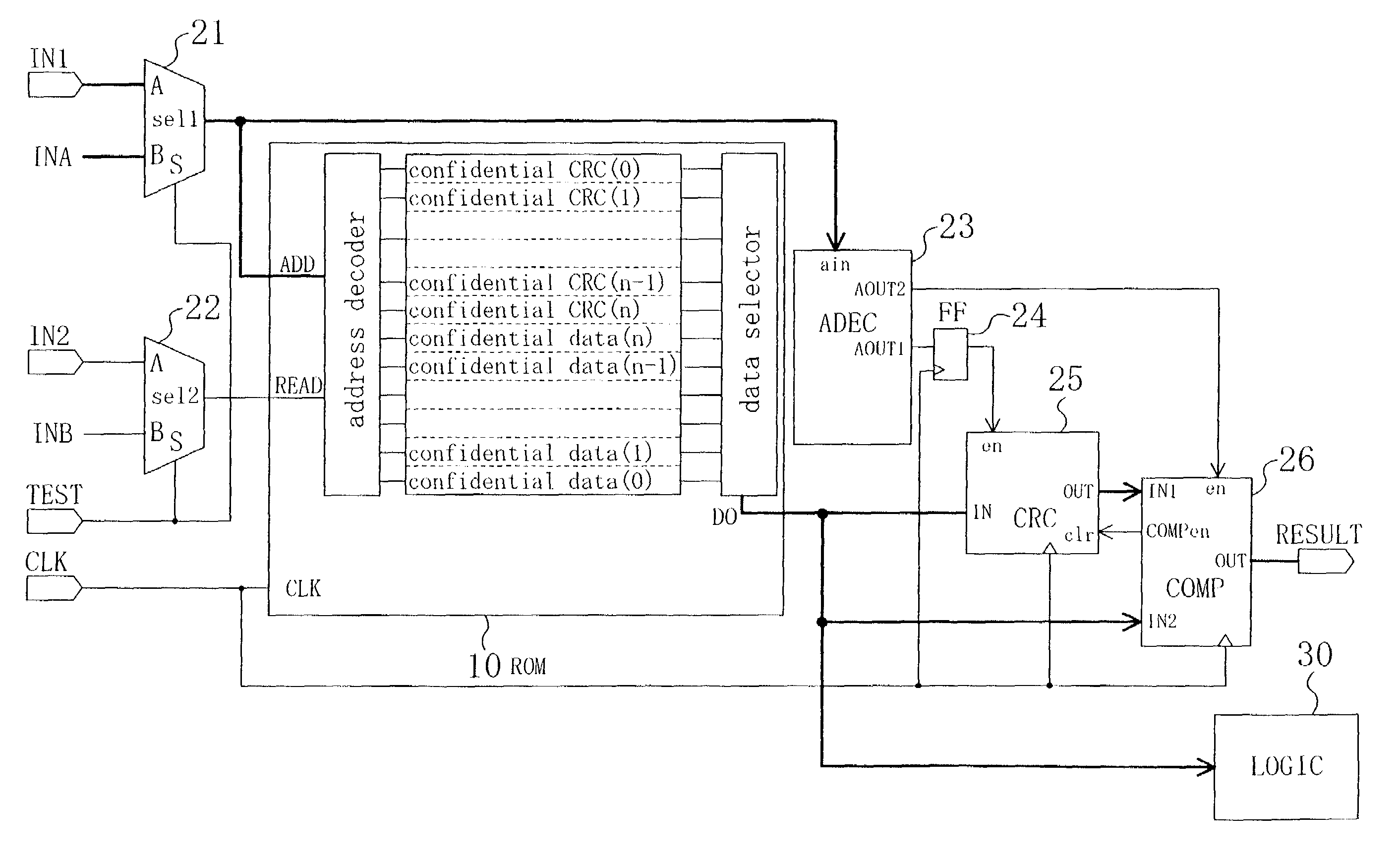
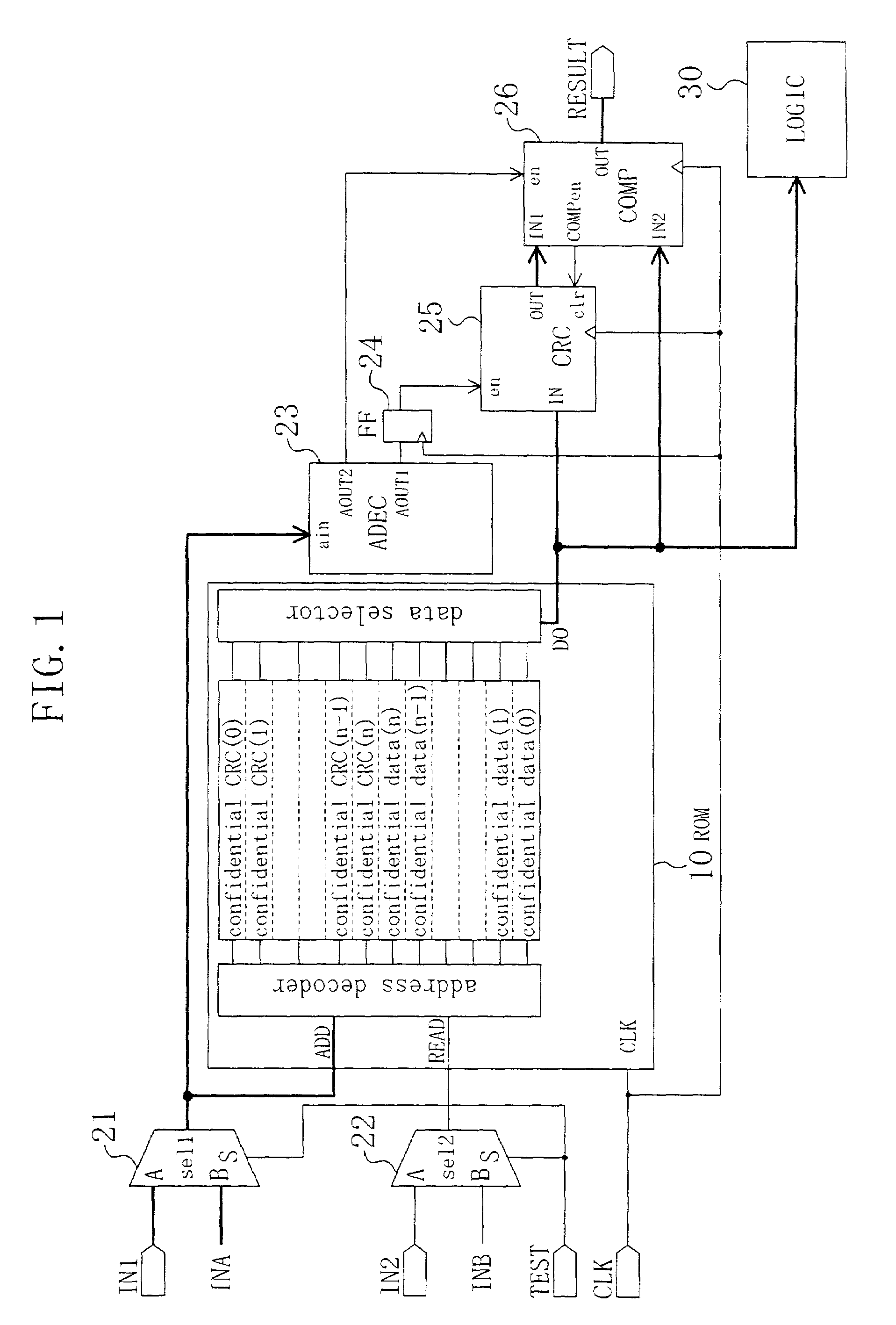
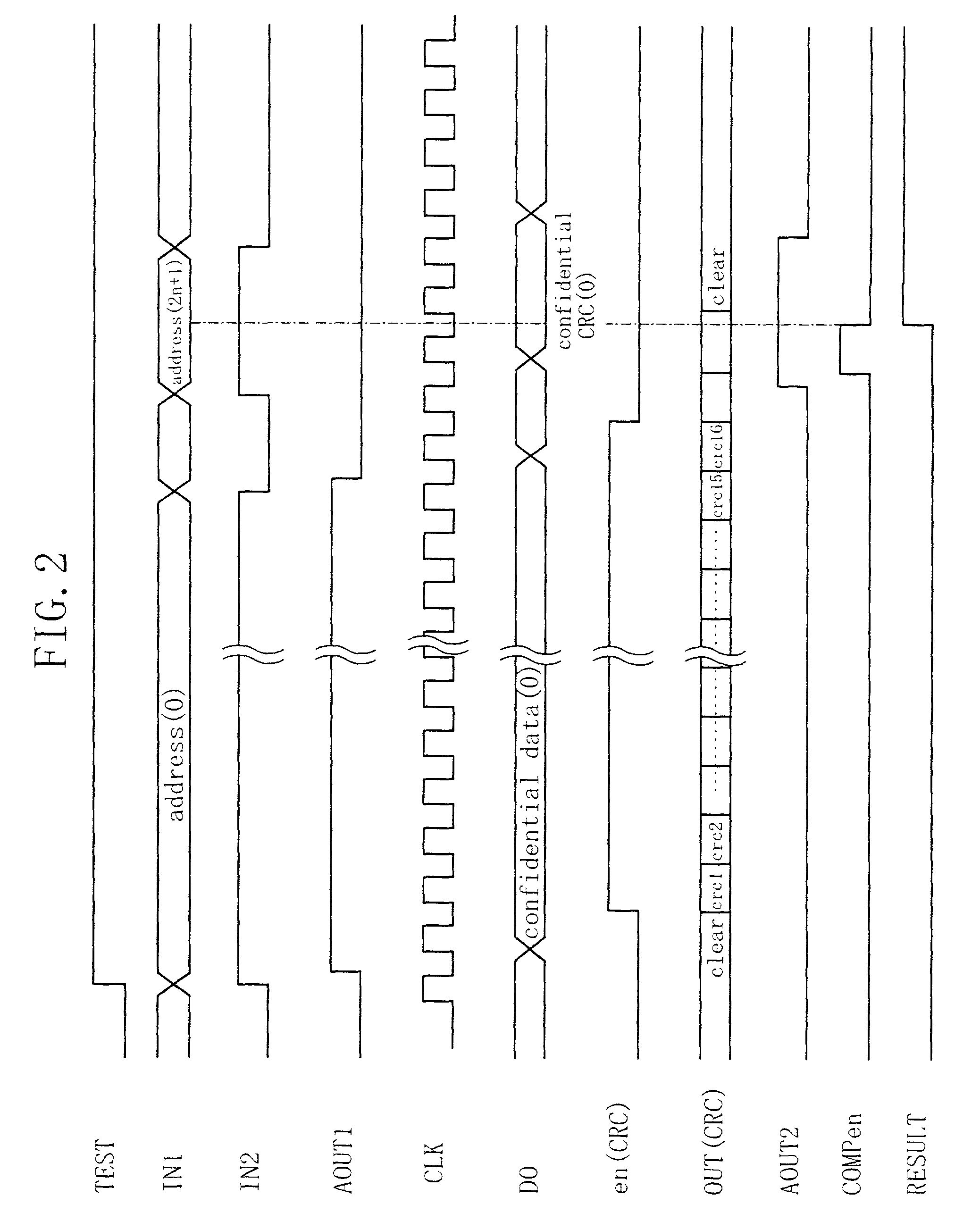
[0018]FIG. 1 illustrates a configuration for a semiconductor integrated circuit according to an embodiment of the present invention. The integrated circuit shown in FIG. 1 can test the ROM 10 without decreasing the security level of confidential information such as microcode, secret keys and passwords.

[0019]As shown in FIG. 1, a number (n+1) of confidential data words (0) through (n) are stored at respective low-order addresses of the ROM 10. Confidential CRC (cyclic redundancy check) codewords (0) through (n), which are equivalent to the “redundancy check data” as defined in the appended claims, have also been produced for the respective confidential data words (0) through (n) and are stored at respective high-order addresses of the ROM 10. In the example illustrated in FIG. 1, the ROM 10 includes the “redundancy check data storage means” as defined in the...


PUM


Abstract

Confidential CRC codewords are stored along with confidential data words on a ROM. A checker subjects one of the confidential data words, which has been read out from the ROM, to the same type of calculation as a predetermined calculation that was carried out to produce associated one of the confidential CRC codewords. A comparator compares a result of the calculation performed by the checker to the associated confidential CRC codeword that has been read out from the ROM.

Description

BACKGROUND OF THE INVENTION[0001]The present invention relates to a technique of testing a ROM that is built in a semiconductor integrated circuit.[0002]FIG. 4 illustrates a configuration for a known ROM-built-in semiconductor integrated circuit with a tester. The circuit shown in FIG. 4 includes selectors 61 and 62 connected to the input terminals of a ROM 51 and another selector 63 connected to the output terminal of the ROM 51. The tester is made up of these three selectors 61, 62 and 63. When a test signal TEST received at an input terminal S is in logical one state (which will be herein referred to as “at H-level”), each of these selectors 61, 62 and 63 selects and outputs a signal received at another input terminal A.[0003]In testing the ROM 51, the test signal TEST is asserted to H-level and supplied to the respective input terminals S of the selectors 61, 62 and 63. Then, input data received at external input terminals IN1 and IN2 are delivered as address and read inputs ADD...

Claims


Application Information

Patent Timeline
Patent Type & Authority Patents(United States)
IPC IPC(8): H04L9/00G06F12/14G06F11/10G06F12/16G06F21/60G06F21/79G11C16/02G11C16/06G11C17/18G11C29/02G11C29/38G11C29/40G11C29/42
CPCG06F11/1004G11C29/42G11C29/40G11C29/38
Inventor FUJIWARA, MAKOTO
Owner PANASONIC SEMICON SOLUTIONS CO LTD
Why Eureka
Try Eureka