
Method for performing timing closure on VLSI chips in a distributed environment

a technology of vlsi chips and distributed environment, which is applied in the direction of computer aided design, program control, instruments, etc., can solve the problems of change in chip state and inability to achieve initial distribution of resources, and achieve the effect of improving the quality of the final resul

Inactive Publication Date: 2007-02-13
IBM CORP
View PDF4 Cites 19 Cited by
  • Summary
  • Abstract
  • Description
  • Claims
  • Application Information

AI Technical Summary

Benefits of technology

[0015]It is still another object to provide a method that employs soft hierarchical boundaries for both physical and timing resources in order to improve the quality of the final result, (e.g., the timing information at the hierarchical boundaries remains in flux throughout the optimization process and the physical locations of circuits in a given partition are not constrained to stay within a specified region, allowing for physical representations of various partitions to overlap with one another, freely spanning across the entire chip).

Problems solved by technology

The problem is partitioned along hierarchical lines, each process owning a single partition within the hierarchy.
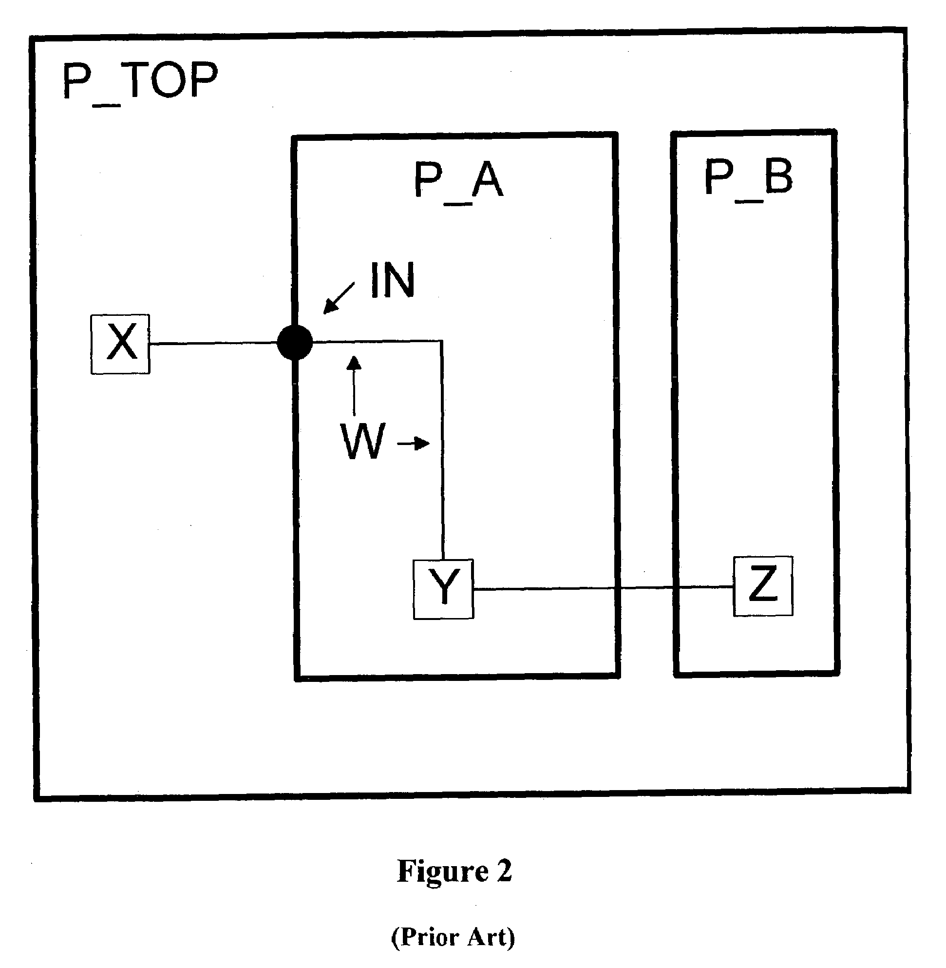
However, as each process optimizes its individual partition, the state of the chip changes and the initial distribution of resources may no longer be desirable.

Method used


Image

  • Method for performing timing closure on VLSI chips in a distributed environment
  • Method for performing timing closure on VLSI chips in a distributed environment
  • Method for performing timing closure on VLSI chips in a distributed environment

Examples


Embodiment Construction

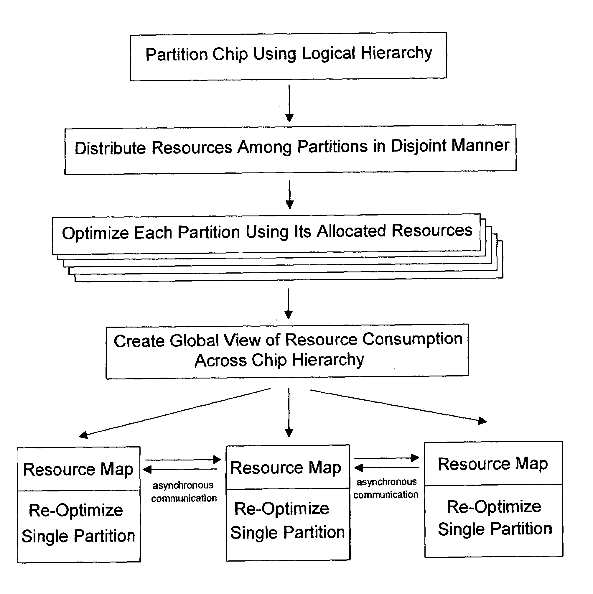
[0026]The inventive method described hereinafter follows the sequence of basic steps illustrated in FIG. 3.[0027]1. The process begins with a hierarchical design. A small number of partitions implies that the size of the average partition is large and, thus, will impact the run time. As the number of partitions increases, the sub-problem size may decrease, although the communication complexity will increase.[0028]2. An initial distribution of physical and timing resources is performed. This initial distribution is in the form of hard hierarchical boundaries designed to bring about a near optimal result. The resources are allocated in a disjoint manner that allows each partition to be optimized independently from each other.[0029]3. Each partition is processed in parallel using the initial fixed resource allocation. The purpose of this step is to bring the chip as close to the final result as possible. However, the inflexible hierarchical boundaries may have prevented timing closure....


PUM


Abstract

A method for performing timing closure on VLSI chips in a distributed environment is described. Abstracting the physical and timing resources of a chip and providing an asynchronous method of updating that abstraction allows multiple partitions of a chip to be optimized concurrently. A global view of physical and timing resources is supplied to local optimizations which are applied concurrently to achieve timing closure. Portions of the hierarchy are optimized in separate processes. Partitioning of the chip is performed along hierarchical lines, with each process owning a single partition in the hierarchy. The processes may be executed by a single computer, or spread across multiple computers in a local network. While optimizations performed by a single process are only applied to its given portion of the hierarchy, decisions are made in the context of the entire hierarchy. These optimizations include placement, synthesis, and routing. The present method can also be expanded to include other resources, such as routing resource, power supply current, power / thermal budget, substrate noise budget, and the like, all of which being able to be similarly abstracted and shared.

Description

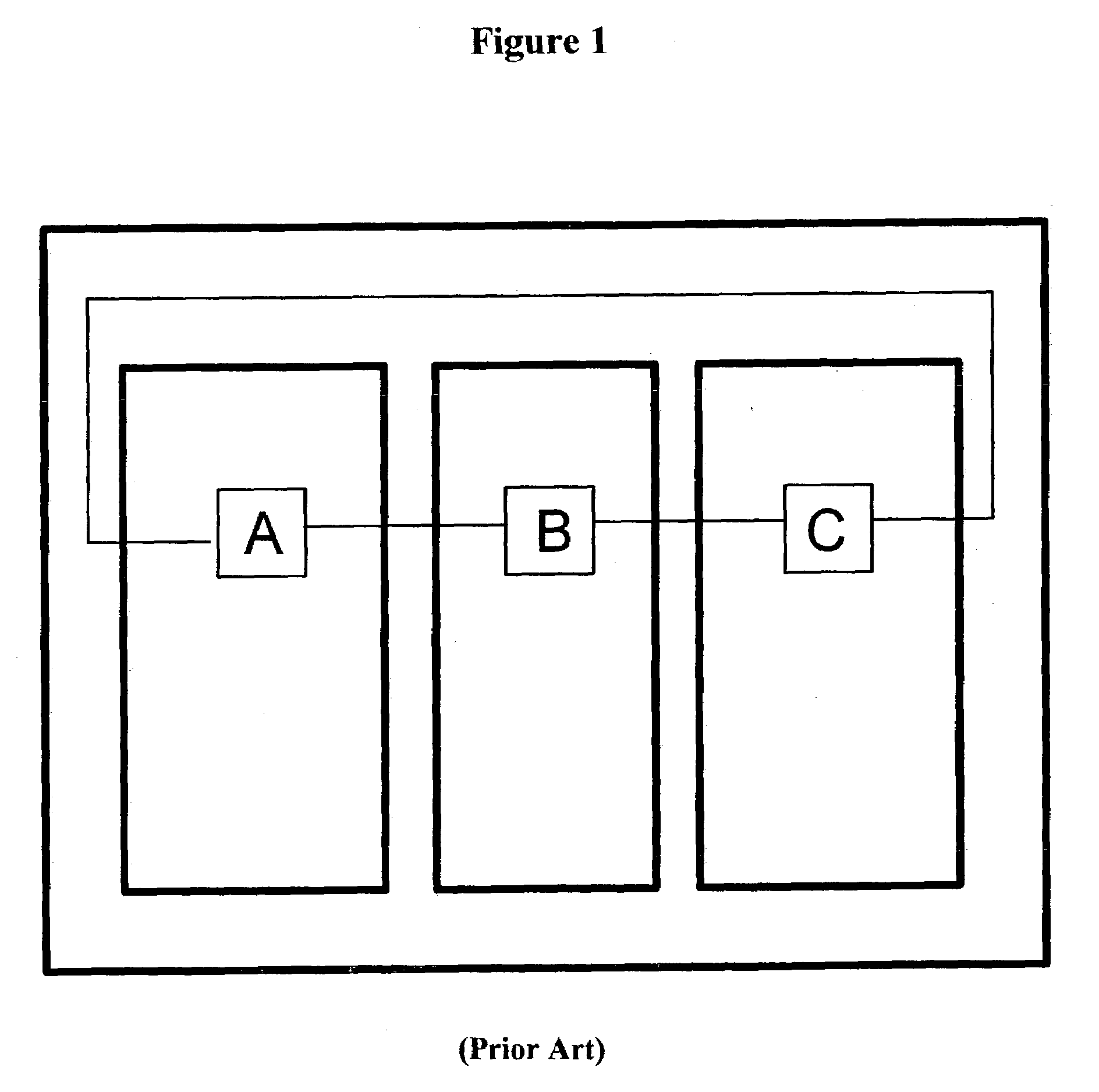
FIELD OF THE INVENTION[0001]This invention is related to conducting a distributed optimization of a partitioned data model by reallocation of physical and timing resources, and more particularly, to a method for achieving timing closure on VLSI chips in a distributed environment.BACKGROUND OF THE INVENTION[0002]The problem of timing closure of Very Large Scale Integrated (VLSI) chips or integrated circuits involves the combination of logic synthesis algorithms with placement and routing algorithms in order to meet timing, area, and other design objectives for the chip. Logic synthesis algorithms change the type and connectivity of circuits used to implement the functionality of the chip. Placement algorithms alter the physical locations of the circuits on the chip. Routing algorithms modify the wire type and path of the connections between the circuits. As the size of the VLSI chips grows, the problem of timing closure increases correspondingly at a geometric rate. A hierarchical ch...

Claims


Application Information

Patent Timeline
Patent Type & Authority Patents(United States)
IPC IPC(8): G06F17/50G06F9/45
CPCG06F17/5072G06F17/505G06F30/327G06F30/392
Inventor HIETER, NATHANIELHATHAWAY, DAVID J.KUDVA, PRABHAKARKUNG, DAVID S.STOK, LEON
Owner IBM CORP
Learn More