
Display memory, driver circuit, display, and cellular information apparatus

a driver circuit and display memory technology, applied in the field of display memory, driver circuit, display, and cellular information apparatus, can solve the problems of increasing the number of drive devices, increasing the power consumption accordingly, and causing the increase of power consumption, so as to reduce the power consumption and achieve high speed

Inactive Publication Date: 2007-02-13
SONY GRP CORP
View PDF11 Cites 70 Cited by
  • Summary
  • Abstract
  • Description
  • Claims
  • Application Information

AI Technical Summary

Benefits of technology

The solution reduces power consumption, enables high-speed graphics drawing, and supports moving picture displays with quick screen switching by optimizing memory access and minimizing the number of memory operations, thereby improving overall display performance.

Problems solved by technology

In conventional liquid crystal drivers, the power consumption of the logic circuits inside the LSI has been lowered by a variety of methods, but if dealing with the enlargement of size of screens or colorization and other improvements in image quality, the number of drive devices increases, so the power consumption rises accordingly.
The operating power consumption of the memory is proportional to the number of times of read / write operations, therefore consequently an increase of the power consumption is induced.
For example, when desiring to display one screen's worth of data stored in a memory on an LCD display screen, (one screen's worth of number of pixels) / (group of pixels) of read operations of the memory become necessary, so there is the disadvantage that power of the amount of the number of times of access is consumed.
Therefore, there is a disadvantage that this is not suited display of a moving picture requiring quick switching of the screen.
For this reason, there were the disadvantages that the number of operation was large and power was consumed.
In this way, conventionally, since a DAC was necessary for every RGB data, the number of DACs was large and an increase of the power consumption was induced.
The phase of the data cannot be freely changed to match with the characteristics of the DACs, so this necessity could not be coped with.
When the operating power supply voltage becomes smaller than 3.0V, however, malfunctions occur.
Further, for a method of supplying power considering power conservation, there is a partial display mode used in a standby screen of mobile phones, but in this partial display mode, although nothing is displayed on the screen, leakage current of the memory cells still flows, so there is the disadvantage of consumption of power.

Method used


Image

  • Display memory, driver circuit, display, and cellular information apparatus
  • Display memory, driver circuit, display, and cellular information apparatus
  • Display memory, driver circuit, display, and cellular information apparatus

Examples


first embodiment

[0066

[0067]FIG. 1 is an overall view of the configuration of a first embodiment of a display 1 according to the present invention. Here, the explanation will be given by taking as an example a liquid crystal driver and a liquid crystal display using the liquid crystal driver circuit.

[0068]In the liquid crystal display 1 shown in FIG. 1, a processor (CPU) 2 for controlling the operation of the entire device, a liquid crystal driver 3, a display screen 4 (liquid crystal panel 4 in the case of a liquid crystal display) for displaying an image, and a scanning circuit 5 for selecting a row of pixels, to which addresses are given in a horizontal direction of the liquid crystal panel 4, and supplying voltage to pixels to turn them on are included.

[0069]The liquid crystal driver 3 has a display memory 7, a CPU side interface (CPU I / F) 6 for receiving the data for every pixel from the CPU 2 and writing the same into the display memory 7 or reading the pixel data stored in the display memory ...

second embodiment

[0113

[0114]In the second embodiment, an example where the power consumption is further reduced by dividing the power supply of the memory and independently providing power to different image data regions of the memory will be explained.

[0115]The display memory in the second embodiment has the configuration of the display memory of the first embodiment. Further, in the second embodiment, the display memory is divided into a plurality of regions, and ON / OFF state of the power is controlled for every separated region or operation mode.

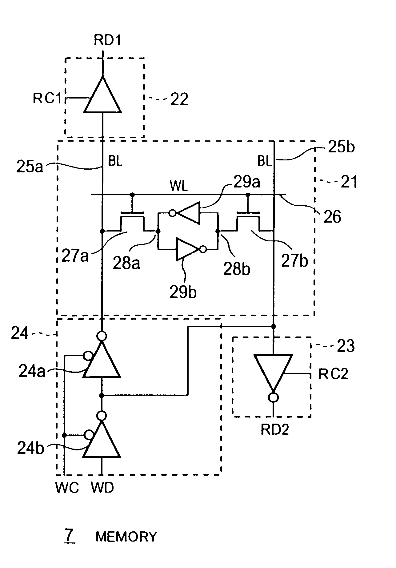
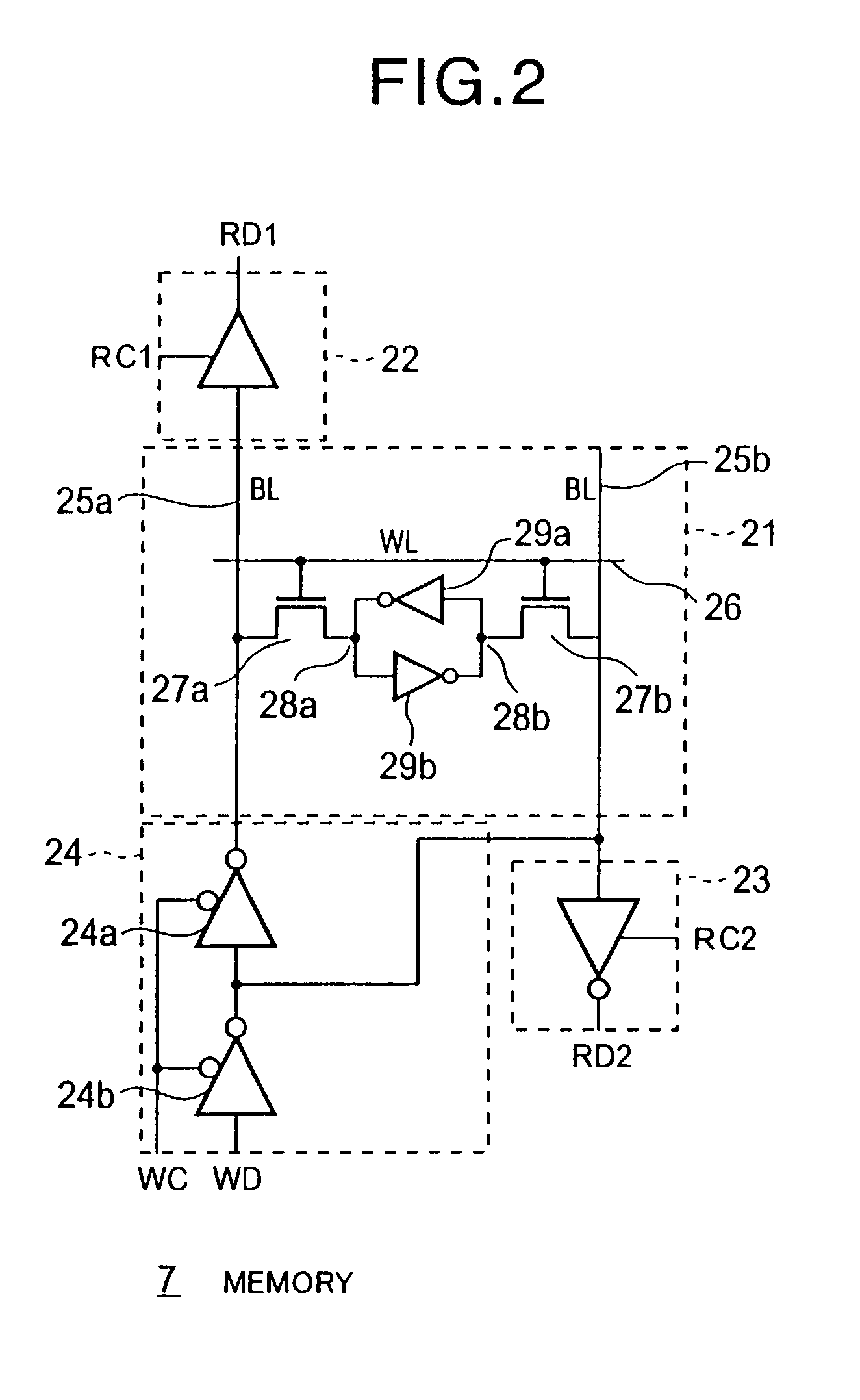
[0116]FIG. 5 is a circuit diagram of the configuration of a display memory dividing the power supply.

[0117]In FIG. 5, the same reference numerals are used for part of the components the same as those of FIG. 2.

[0118]In FIG. 5, 51a, 51b, and 51c indicate memory cells of the display memory 7 according to the first embodiment shown in FIG. 2, 52a and 52b indicate a pair of bit lines (BL), 53a, 53b and 53c indicate word lines (WL), 54a, 54b, and 54c indicate ...

third embodiment

[0136

[0137]The display memory according to the third embodiment has a similar basic configuration to that of the display memory of the first embodiment. Note, in the third embodiment, the address array of the display memory corresponds to the pixel array of the liquid crystal panel so the image of the image data stored in the display memory becomes the same as the screen of the liquid crystal panel. Further, the read or write access with respect to the display memory is carried out in units of one row's worth of the pixel data on the screen.

[0138]FIG. 6 is a schematic view of the address array of the display memory and the array of pixels of the liquid crystal panel according to the third embodiment.

[0139]In FIG. 6, the address array of the memory and the pixel matrix of the liquid crystal panel are expressed by an array having lines ln0 to lnN and pixels px0 to pxN as suffixes. The arrays of addresses of the memory and pixels of the liquid crystal panel become the same in image. Na...


PUM

PropertyMeasurementUnit
voltageaaaaaaaaaa
diagonal lengthaaaaaaaaaa

Abstract

A display memory able to reduce power consumption, able to generate graphics at a high speed, and not needing memory mapping, a driver circuit, a display using the driver circuit, and a portable information apparatus, wherein a CPU read circuit is connected to one bit line of a display memory 7, a display read circuit is connected to the other bit line, a write circuit is connected to both bit lines, the CPU read circuit and write circuit are assigned to the access from the CPU, the display read circuit is assigned to the display screen display, and further the access from the CPU and the reading to the display screen are assigned to different two level periods of a clock signal of the memory and independently controlled. Further, a drive power supply of the display memory is divided and a drive power supply voltage is supplied to the display memory for every memory cell or for every plurality of memory cells.

Description

BACKGROUND OF THE INVENTION[0001]The present invention relates to a display memory for storing pixel data to be supplied to pixels of a display, a driver circuit having a display memory and driving pixels arrayed in a matrix of the display by signals corresponding to the image data, a display using the driver circuit, and a portable information device.[0002]Liquid crystal displays are being widely used as display systems of mobile phones and PDAs (Personal Digital Assistants) and other portable information devices by making use of their light weight, thinness, low power consumption, and other features. Further, due to the spread of mobile phones and the Internet, the displays of portable information devices are being required to be further enlarged in size, offer color, and otherwise be improved in quality and are being strongly required to be ultra-low in power consumption for realizing long hours of usage. In liquid crystal drivers, therefore, it has become important to realize lo...

Claims


Application Information

Patent Timeline
Patent Type & Authority Patents(United States)
IPC IPC(8): G09G3/36G02F1/133G09GG09G3/20G09G3/30G09G5/395G11C11/41
CPCG09G3/20G09G3/3685G09G5/393G09G5/395G09G3/2003G09G3/3611G09G5/001G09G2360/126G09G2310/027G09G2310/0297G09G2330/021G09G2330/026G09G2330/027G09G3/36
Inventor MORIYAMA, KATSUTOSHIAYABE, TOMOYAMIZUTA, TAISHI
Owner SONY GRP CORP
Learn More