
Seek window verify program system and method for a multilevel non-volatile memory integrated circuit system

Inactive Publication Date: 2006-12-12
SILICON STORAGE TECHNOLOGY
View PDF4 Cites 54 Cited by
  • Summary
  • Abstract
  • Description
  • Claims
  • Application Information

AI Technical Summary

Problems solved by technology

The mismatch generates a current ratio error and may be caused by mismatches of the threshold voltage, the width, length, mobility, and oxide thickness of the circuit elements, such as transistors, in the signal paths.
The mismatch also may be caused by mismatch in signal paths due to parasitics, such as width and length of interconnects.

Method used


Image

  • Seek window verify program system and method for a multilevel non-volatile memory integrated circuit system
  • Seek window verify program system and method for a multilevel non-volatile memory integrated circuit system
  • Seek window verify program system and method for a multilevel non-volatile memory integrated circuit system

Examples


second embodiment

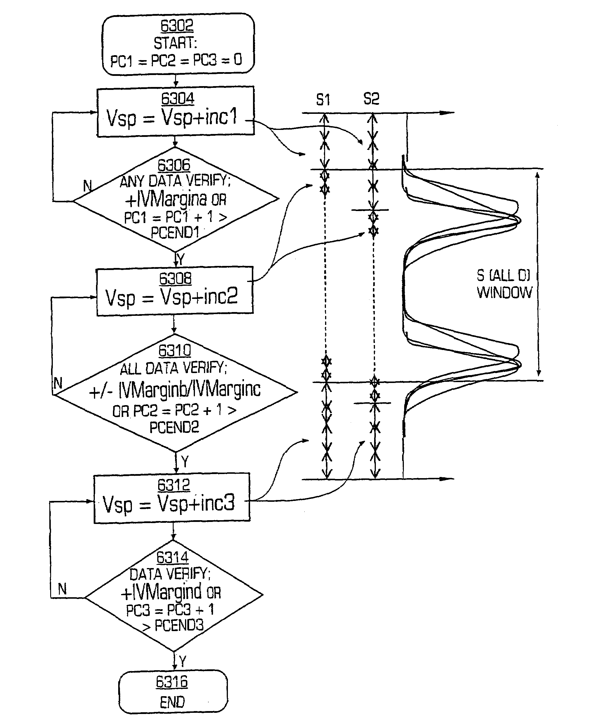
[0479]FIG. 64 is a flow diagram illustrating a seek window and programming procedure in a

[0480]The algorithm controller 164 first seeks a dynamic window of a group of cells (e.g., a sector that may include for example 128 k or 32 k memory cells). The seeking of the window is done by using a combination of variable steps to seek out the first end portion of the window.

[0481]First, second, third, and fourth increment pulse counters are initialized (PC1=PC2=PC3=PC4=0) (block 6402). The programming voltage VSP is incremented by a first incremental voltage (inc1) (block 6404). The data is verified with a first margin (IVMargina) associated with reference level of the first point of the window (block 6406), and if the data is not verified and the first increment pulse counter (PC1) does not exceed a threshold (PC1+1>PCEND1), the first increment pulse counter (PC1) is incremented and the programming voltage is incremented by the first incremental voltage (inc1) (block 6404). If any data is...

third embodiment

[0482]FIG. 65 is a flow diagram illustrating a seek window and programming procedure in a

[0483]The algorithm controller 164 first seeks out a window for individual cells (e.g., D1 or D2) and then applies precision programming for the found data window to achieve precision levels.

[0484]First, second, and third increment pulse counters are initialized (PC1=PC2=PC3=0) (block 6502). The programming voltage VSP is incremented by a first incremental voltage (inctry) (block 6504). The data is verified with a first margin (IVMarginx) associated with the reference level of the first point of the window (block 6506), and if the data is not verified and the first increment pulse counter (PC1) does not exceed a threshold (PC1+1>PCEND1), the first increment pulse counter (PC1) is incremented and the programming voltage is incremented by the first incremental voltage (inctry) (block 6504). If any data is verified or the first increment pulse counter (PC1) exceeds a threshold (PC1+1>PCEND1, all da...

fourth embodiment

[0485]FIG. 66 is a flow diagram illustrating a seek window and programming procedure in accordance with a

[0486]The algorithm controller 164 first seeks out a window for individual cells (e.g., D1 or D2) and then applies precision programming for the found data window to achieve precision levels. The seeking is done by using a combination of small steps and large steps to seek out the first end portion of the window.

[0487]First, second, third, and fourth increment pulse counters are initialized (PC1=PC2=PC3=PC4=0) (block 6602). The programming voltage VSP is incremented by a first incremental voltage (inc1) (block 6604). The data is verified with a first margin (IVMargina) associated with the reference level of the first point of the window (block 6606), and if the data is not verified and the first increment pulse counter (PC1) does not exceed a threshold (PC1+1>PCEND1), the first increment pulse counter (PC1) is incremented and the programming voltage is incremented by the first in...


PUM


Abstract

A memory comprises a plurality of digital multilevel memory cells. A window of valid data voltages for accessing the said plurality of digital multilevel memory cells is detected. The window may be detected by incrementing a first programming voltage to program data in the plurality of memory cells and verifying whether the data in at least one of said plurality of memory cells is properly programmed. The incrementing and verifying may be repeated until data is verified to be properly programmed in one of said plurality of memory cells. The data in each memory cell of said plurality of memory cells is verified. The verification may be by incrementing a second programming voltage, and verifying whether data in each memory cell is properly programmed within a margin. The incrementing and verifying is repeated for each memory cell outside of the margin.

Description

CROSS-REFERENCE TO RELATED APPLICATIONS[0001]This is a continuation-in-part of application Ser. No. 10 / 317,455, filed Dec. 11, 2002 now U.S. Pat. No. 6,959,779, which is a continuation-in-part of application Ser. No. 10 / 211,886, filed Aug. 1, 2002 now U.S. Pat. No. 6,865,099, which is a continuation-in-part of application Ser. No. 09 / 929,542, filed Aug. 13, 2001 now U.S. Pat. No. 6,751,118, which is a division of application Ser. No. 09 / 231,928 filed Jan. 14, 1999, issued as U.S. Pat. No. 6,282,145, the subject matter of each of these applications is incorporated herein by reference.FIELD OF THE INVENTION[0002]This invention relates in general to semiconductor memories, and, in particular, to the design and operation of multilevel nonvolatile semiconductor memories.BACKGROUND OF THE INVENTION[0003]As the information technology progresses, the demand for high density giga bit and tera bit memory integrated circuits is insatiable in emerging applications such as data storage for photo...

Claims


Application Information

Patent Timeline
IPC IPC(8): G11C11/34G11C11/56G11C16/08G11C16/10G11C16/24G11C16/28G11C27/00
CPCG11C11/5621G11C11/5628G11C11/5635G11C11/5642G11C11/5678G11C13/0026G11C13/0028G11C13/004G11C13/0064G11C13/0069G11C16/08G11C16/10G11C16/24G11C16/28G11C27/005G11C13/0004G11C2013/0054G11C2211/5634
Inventor TRAN, HIEU VANNGUYEN, HUNG Q.LEVI, AMITAYNOJIMA, ISAO
Owner SILICON STORAGE TECHNOLOGY
Learn More