
Data inversion circuits having a bypass mode of operation and methods of operating the same

a data inversion circuit and bypass mode technology, applied in the field of integrated circuit devices with high data bandwidth, can solve the problems of deteriorating signal integrity of memory devices, large noise, and simultaneous switching noise (ssn), and achieve the effects of reducing simultaneous switching noise, and reducing read path read latency

Inactive Publication Date: 2006-11-28
SAMSUNG ELECTRONICS CO LTD
View PDF17 Cites 16 Cited by
  • Summary
  • Abstract
  • Description
  • Claims
  • Application Information

AI Technical Summary

Benefits of technology

The present invention relates to an integrated circuit device that includes a data inversion circuit for reducing simultaneous switching noise in a memory device read path. The data inversion circuit includes an inversion unit and a bypass unit that can be selectively enabled or disabled based on a control signal. The control signal is generated based on a delay between receiving a first read instruction and a second read instruction. The data inversion circuit can be selectively enabled or disabled based on a predetermined number of clock cycles or a reset signal. The invention also includes a method for reducing simultaneous switching noise and improving read latency by selectively enabling or disabling the data inversion circuit based on the delay between the first and second read instructions.

Problems solved by technology

In such a high bandwidth memory device, the 32 DQ pins may operate at the same time when data is output, resulting in a great amount of noise, known as simultaneous switching noise (SSN).
Due to SSN, waveforms of data output signals may be distorted, which may deteriorate signal integrity of the memory device.
As such, it may be difficult for the memory device to satisfy the input / output performance required in a high-frequency system.
However, a conventional data inversion circuit may be inefficient in that an inversion operation may be performed on the data to be currently output regardless of the presence of a reading interval between the previous data and the data to be currently output.
Also, such an inversion operation may reduce the operating speed of the semiconductor device.
Such a timing margin may further reduce the operating speed of the data inversion circuit, and may limit the operational frequency of the semiconductor device.

Method used


Image

  • Data inversion circuits having a bypass mode of operation and methods of operating the same
  • Data inversion circuits having a bypass mode of operation and methods of operating the same
  • Data inversion circuits having a bypass mode of operation and methods of operating the same

Examples


Embodiment Construction

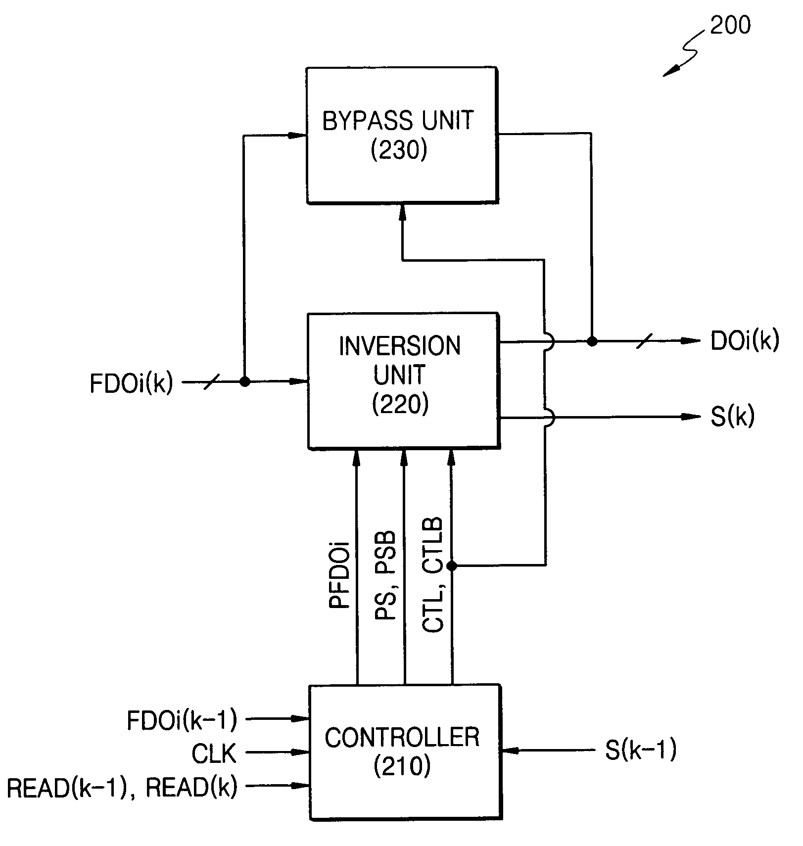
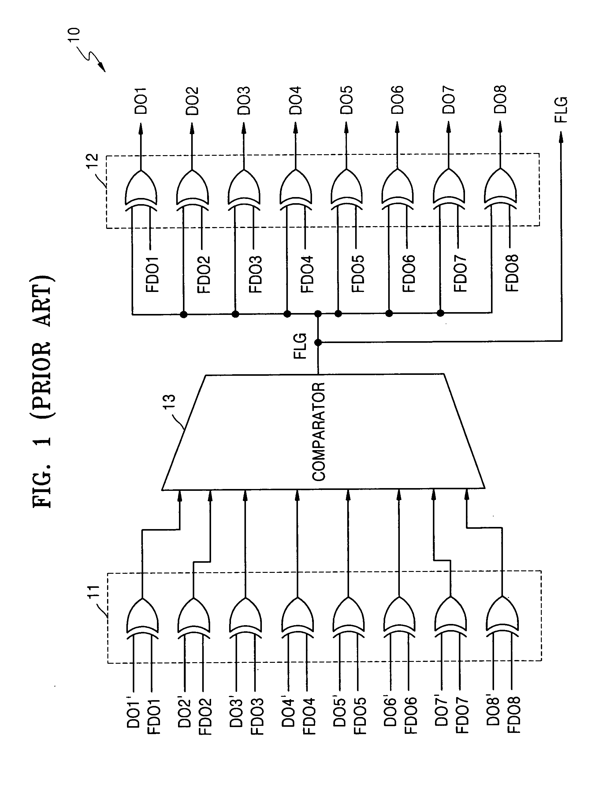
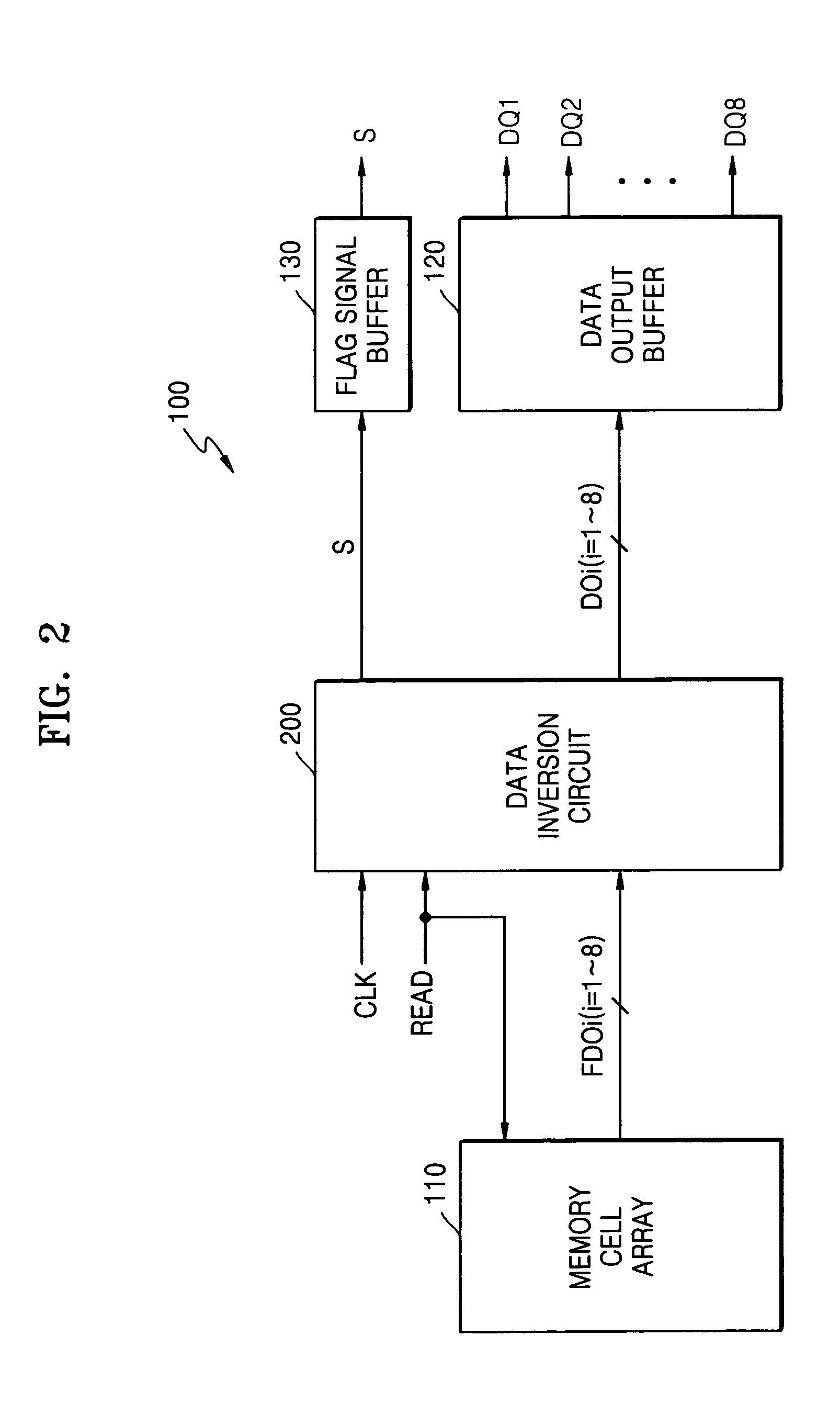
[0044]The present invention now will be described more fully herein with reference to the accompanying drawings, in which preferred embodiments of the invention are shown. This invention may, however, be embodied in many different forms and should not be construed as being limited to the embodiments set forth herein; rather, these embodiments are provided so that this disclosure will be thorough and complete, and will fully convey the scope of the invention to those skilled in the art. Like reference numerals refer to like elements throughout and signal lines and signals thereon may be referred to by the same reference characters. Signals may also be synchronized and / or undergo minor boolean operations (e.g., inversion) without being considered different signals. Moreover, when a device or element is stated as being responsive to a signal(s), it may be directly responsive to the signal(s) or indirectly responsive to the signal(s) (e.g., responsive to another signal(s) that is derive...


PUM


Abstract

An integrated circuit device includes a data inversion circuit configured to support an inversion mode of operation. The inversion mode of operation inverts selected ones of a plurality of N-bit words received in consecutive sequence at inputs thereof. The data inversion circuit is further configured to support a bypass mode of operation. The bypass mode of operation disables inversion of a second one of the plurality of N-bit words when a delay between receipt of the second one of the plurality of N-bit words and receipt of an immediately preceding first one of the plurality of N-bit words is greater than a predetermined time interval. Related methods are also discussed.

Description

REFERENCE TO PRIORITY APPLICATION[0001]This application claims priority to Korean Patent Application No. 2003-90940, filed on Dec. 13, 2003, the disclosure of which is hereby incorporated by reference herein in its entirety.CROSS-REFERENCE TO RELATED APPLICATIONS[0002]This application is related to commonly assigned U.S. patent application Ser. No. 10 / 815,505, filed Apr. 1, 2004, the disclosure of which is hereby incorporated herein by reference. This application is also related to commonly assigned U.S. Pat. No. 6,788,106, filed Mar. 26, 2003, the disclosure of which is hereby incorporated by reference herein.BACKGROUND OF THE INVENTION[0003]1. Field of the Invention[0004]The present invention relates to integrated circuit devices, and more particularly, to integrated circuit devices having high data bandwidth..[0005]2. Description of the Related Art[0006]Generally, semiconductor memory devices have a high bandwidth input / output (I / O) structure, and may include 32 data output pins,...

Claims


Application Information

Patent Timeline
Patent Type & Authority Patents(United States)
IPC IPC(8): H03K19/20G11C7/10H03K19/003
CPCH03K19/00346H03K19/00361G11C7/10
Inventor PARK, MIN-SANG
Owner SAMSUNG ELECTRONICS CO LTD
Learn More