
Photodiode

a photodiode and photodiode technology, applied in the field of photodiodes, can solve the problems of reducing affecting the detection accuracy of readouts, and affecting the accuracy of readouts, so as to reduce the bandwidth of photodiodes, reduce the cost of detecting diffusion currents, blur the response of photodiodes

Active Publication Date: 2006-11-28
MAGNOLIA LICENSING LLC
View PDF21 Cites 3 Cited by
  • Summary
  • Abstract
  • Description
  • Claims
  • Application Information

AI Technical Summary

Benefits of technology

[0012]It is the object of the present invention to provide a photodiode enabling a faster read-out.
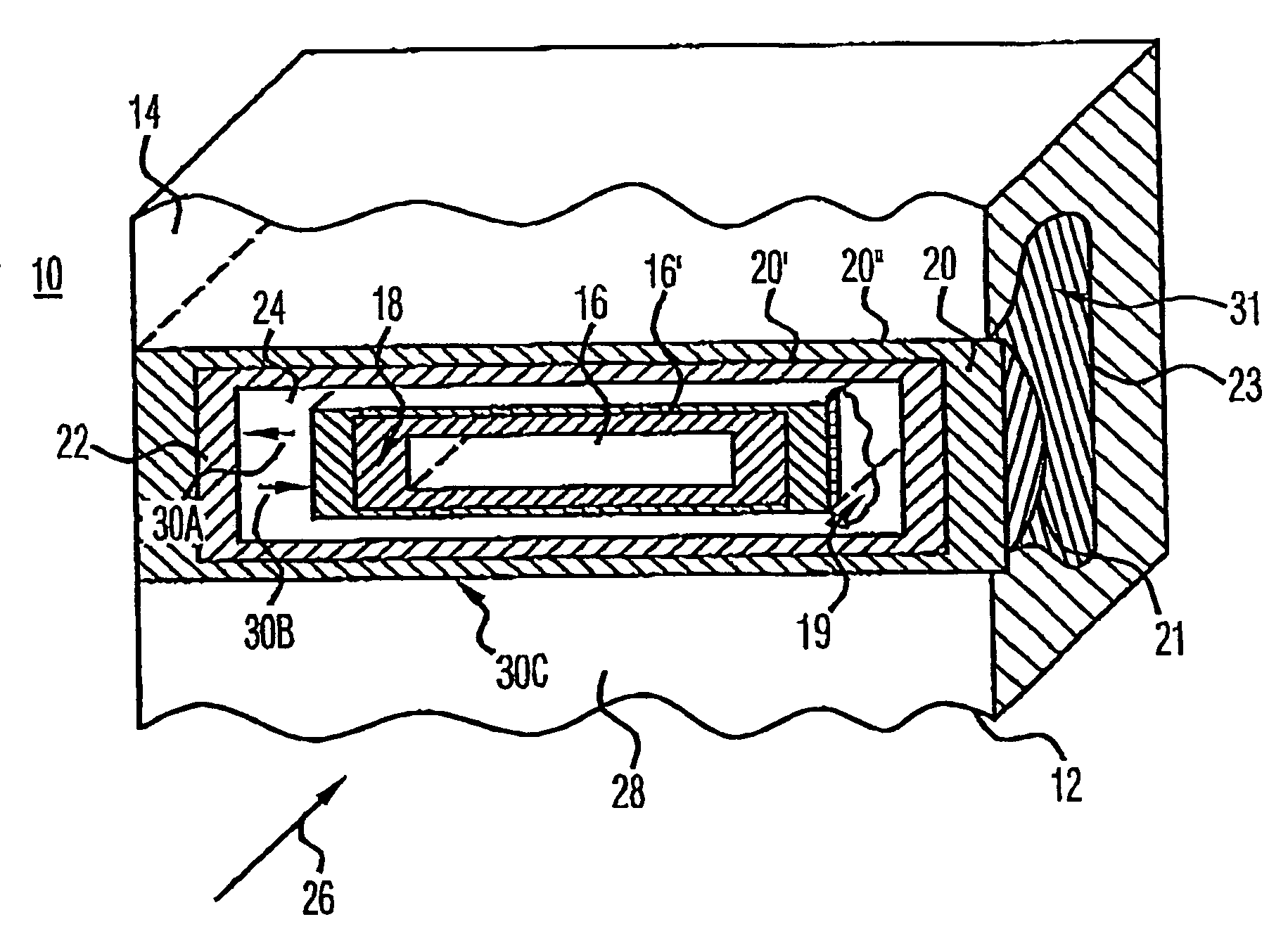
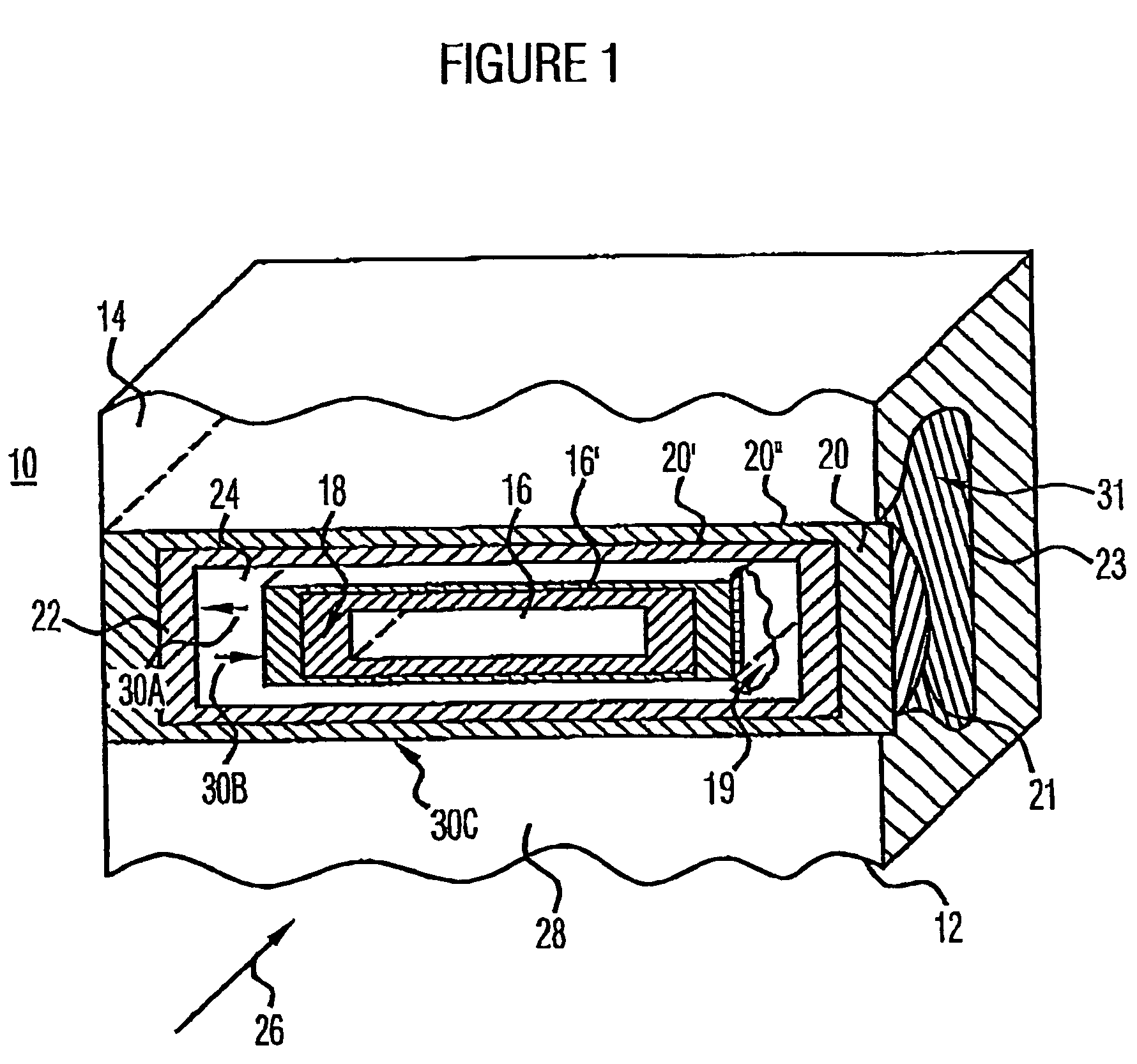
[0015]The present invention is based on the finding that decreasing the bandwidth of photodiodes by blurring the response of the photodiode by the diffusion current can be reduced by providing insulation means in the semiconductor substrate, which localizes the diffusion region with regard to the adjacent semiconductor substrate and reduces the number of charge carriers contributing to the diffusion portion, on the one hand, by decreasing the diffusion region in which the diffused charge carriers are generated and, on the other hand, by “sucking” diffusing charge carriers generated in the smaller diffusion region by means of the insulation means, which is why they do not contribute to the photocurrent.
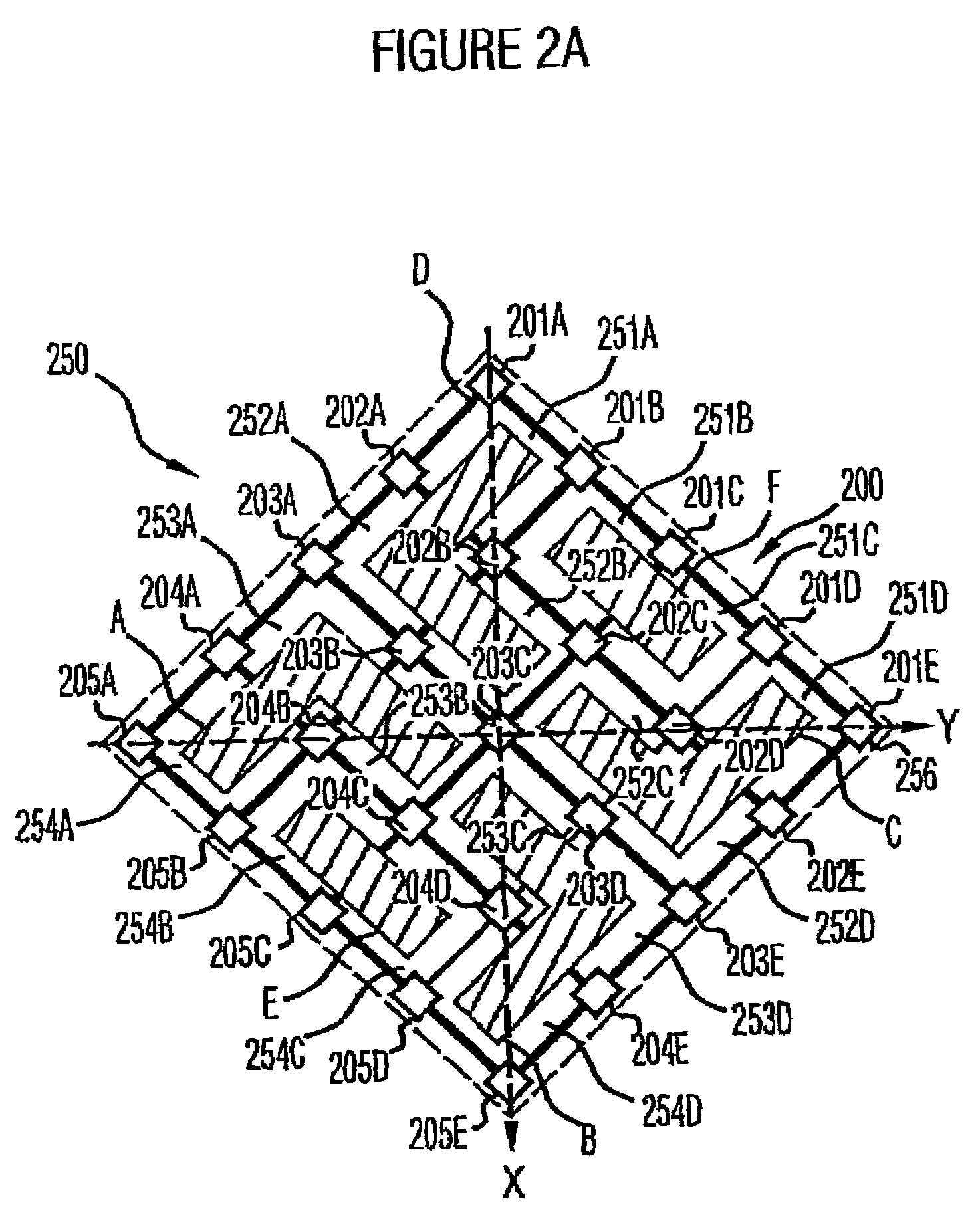
[0016]In accordance with an embodiment of the present invention, the semiconductor substrate is of a first conductivity type, the space-charge zone region is formed by a signal region having a second conductivity type in the semiconductor substrate and the insulation means is formed by an insulation region of a second conductivity type in the semiconductor substrate in a predetermined spacing to the signal region. In a special embodiment of the present invention where a plurality of photo-sensitive regions are arranged as a photodiode array, insulation regions are arranged such that they localize every photodiode formed by a respective photo-sensitive region with regard to its diffusion region and shield each photo-sensitive region of a photodiode from charge carriers diffusing from a neighboring diffusion region of a neighboring photodiode. The insulation regions in the semiconductor substrate form space-charge zones and thus themselves form detecting diodes also used for read-out. In this way, an array of fast photodiodes having a small diffusion and a large drift current portion, which subsequently will be referred to as RF diodes, is formed, the array being interspersed by an array of slow detection diodes having a high diffusion current portion, which subsequently will be referred to as LF diodes. Another advantage is that the sensitivity characteristic curve of the photodiode is made constant over the wavelength with a simultaneous read-out of the photocurrent provided by the RF diodes and of the photocurrent generated by the LF diode formed by the insulation region.

Problems solved by technology

Apart from the expenses for the external devices, this causes further expenses for example due to additional casing pins, bond pads, high-area and high-current input / output interfaces and additional printed circuit board area.
The disadvantage of this procedure is that about half of the light power is employed for detecting the diffusion current.
Furthermore, there are several non-amplifying devices in the signal path, which in turn means a considerable deterioration of the noise features of the read-out.
In particular in communications and optical memory systems, noise is a critical parameter so that the procedure used there can only be employed in such systems under certain circumstances.
Another disadvantage of prior-art photodiodes generated on the process level is that they exhibit, as has been described before, a sensitivity characteristic curve which depending on the wavelength is not constant.

Method used


Image

  • Photodiode
  • Photodiode
  • Photodiode

Examples


Embodiment Construction

[0032]FIG. 1 shows an embodiment of a photodiode generally indicated by 10. The photodiode includes a substrate of a first conductivity type, such as, for example, p-doped, which is generally indicated by 12 and comprises a main surface 14 which in FIG. 1, which is designed as a partial sectional spatial illustration, can be seen head-on. In the semiconductor substrate 12, a signal region 16 of a second conductivity type opposite to the first one is formed, such as, for example, n-doped, wherein the perimeter thereof is indicated in FIG. 1 by 16′. The signal region 16 abuts on the main surface 14 and extends to a certain depth into the substrate. A space-charge zone region 18 which in FIG. 1 is illustrated in a hatched manner and extends along the perimeter 16′ of the signal region 16 both into the signal region 16 and from there into the semiconductor substrate 12 is formed by the signal region 16 of the second conductivity type in the semiconductor substrate 12 of the first conduc...


PUM


Abstract

Apart from a semiconductor substrate and a photosensitive region in the semiconductor substrate, which comprises a space charge zone region for generating a diffusion current portion and a diffusion region for generating a diffusion current portion, a photodiode includes an insulation means in the semiconductor substrate for at least partially confining the diffusion region against an adjacent surrounding region of the semiconductor substrate. The reduction of the bandwidth of photodiodes by the smearing of the response of the photodiode by the diffusion current is alleviated by providing an insulation means in the semiconductor substrate, which confines the diffusion region against the surrounding semiconductor substrate and hereby on the one hand reduces the number of charge carriers contributing to the diffusion portion by reducing the diffusion region, in which the diffusing charge carriers are generated, and on the other hand by “sucking off” diffusing charge carriers generated in the shrunk diffusion region by the insulation means, which is why same do not contribute to the photocurrent.

Description

CROSS-REFERENCE TO RELATED APPLICATION[0001]This application is a continuation of co-pending International Application No. PCT / EP03 / 05378, filed May 22, 2003, which designated the United States and was not published in English and is incorporated herein by reference in its entirety.BACKGROUND OF THE INVENTION[0002]1. Field of the Invention[0003]The present invention relates to a photodiode and, in particular, to fast photodiodes as are, for example, utilized in optical memories and in optical communications.[0004]2. Description of the Related Art[0005]Photodiodes are applied in various fields. Photodiodes are, for example, employed in X-ray detectors, camera sensors, triangulation sensors, optocouplers, monitoring devices, optical memories and optical transmission systems. In particular in the last-mentioned fields of application, photodiodes enabling signal processing in the megahertz to gigahertz region are required.[0006]A photodiode utilizes the electrical field of a pn junction...

Claims


Application Information

Patent Timeline
IPC IPC(8): H01L31/0328H01L27/144H01L31/04H01L27/146H01L27/15H01L31/0352H01L31/103
CPCH01L27/1463H01L31/035281H01L27/14643H01L31/103Y02E10/50Y10S257/927
Inventor HEHEMANN, INGOKEMNA, ARMIN
Owner MAGNOLIA LICENSING LLC
Learn More