
Fabrication method of multisensors chips for detecting analytes

Inactive Publication Date: 2006-11-21
UNIV ROVIRA I VIRGILI
View PDF2 Cites 1 Cited by
  • Summary
  • Abstract
  • Description
  • Claims
  • Application Information

AI Technical Summary

Benefits of technology

[0033]An additional advantage of the invention method is that it allows selective deposition of the (bio)chemical recognition element, with photolithographic resolution, in short periods of time, generally between 1 and 5 minutes as every cycle of the invention method can be done in very low periods of time. In a particular performance, each cycle of the invention method can be done in periods of time less than 120 seconds, including the deposition and washing stages. Consequently, the fabrication process can be completed at speeds comparable to the contact and non-contact printing techniques.
[0034]The following examples illustrate the invention and should not be considered as indicating its limit.

Problems solved by technology

The disadvantage of this technique is that there is no possibility for the control of quality of the synthesised probes and, consequently, a redundancy in the number of hybridisation sites is necessary to assure reliability.
Ideally, the resolution of these techniques is also limited by the photolitographic limit of the design of the array.
Consequently, they are more advantageous than the techniques previously mentioned, but, maybe, require more time for their design and might present the drawback of non-selective deposition.
In addition, liquid chemistry is used for the production, which is not a standard in the semiconductor industry.
However, none of these previous articles mentions the possibility of selective deposition with micrometric or sub-micrometric resolution.

Method used


Image

  • Fabrication method of multisensors chips for detecting analytes
  • Fabrication method of multisensors chips for detecting analytes
  • Fabrication method of multisensors chips for detecting analytes

Examples


example 1

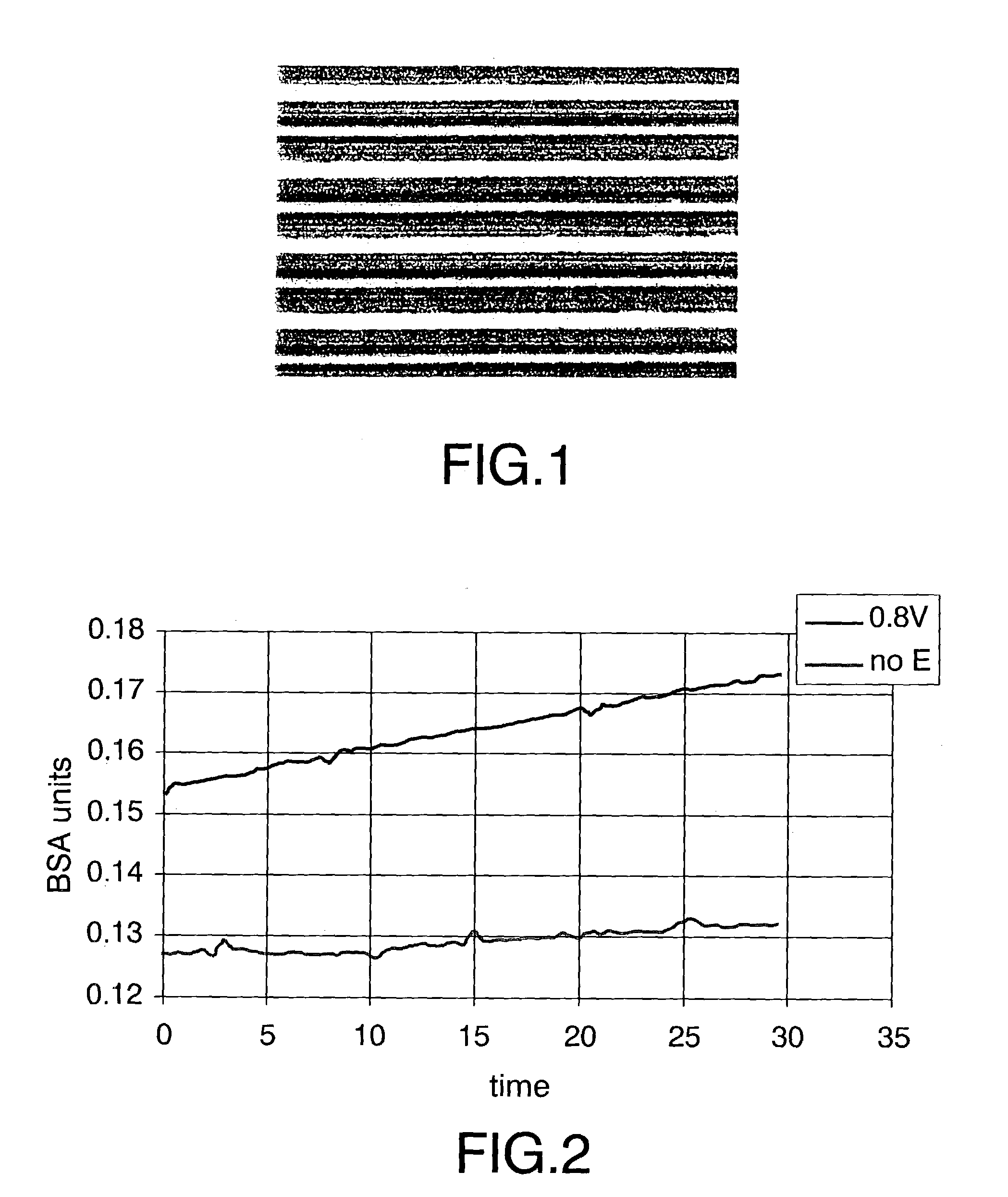
[0035]This example illustrates the selective deposition of conjugates FOTCG in one of the electrodes that constitutes an interdigitated array. For this purpose, a solution of a FOTCG conjugate obtained according to the protocol described by Storhoff and collaborators [Storhoff et al. (1998), Journal of the American Chemical Society, 120:1959–1964], was put in contact with said interdigitated array and a +1.6V (vs. Ag / AgCl sat'd) potential was applied for two hours on half of the electrodes of the array. The selective deposition of these conjugates over the electrodes on which the potential was applied was characterised by optical microscopy. The results obtained are shown in FIG. 1 on which lines of different colours can be seen, specifically:[0036]grey lines (5 μm of thickness), which correspond to the interspace between electrodes;[0037]yellow lines (5 μm of thickness), which correspond to the electrode on which potential has not been applied; and[0038]orange lines (5 μm of thickn...

example 2

[0040]This example illustrates the selective deposition of colloidal gold on transparent electrodes of ITO. For this purpose, a colloidal gold suspension [Sigma, reference: G-1652 (gold colloid, 20 nm)] was put in contact with the ITO transparent electrodes. The deposition was done applying +0,8V (vs. Ag / AgCl saturated) for 30 minutes. As control were used electrodes on which potential was not applied. The colloidal gold deposition on the electrodes was characterised by spectrophotometry, monitoring in real time the absorbance at the colloidal gold characteristic wavelength (523 nm), deposited on the electrode. The obtained results are shown in FIG. 2, on which a more pronounced slope can be observed corresponding to the electrode on which potential was applied (0.8V), indicating the colloidal gold selective deposition in that electrode compared to the control (not polarised).

example 3

[0041]This example illustrates the selective deposition of DOTCG conjugates on electrodes obtained through the screen printing technique.

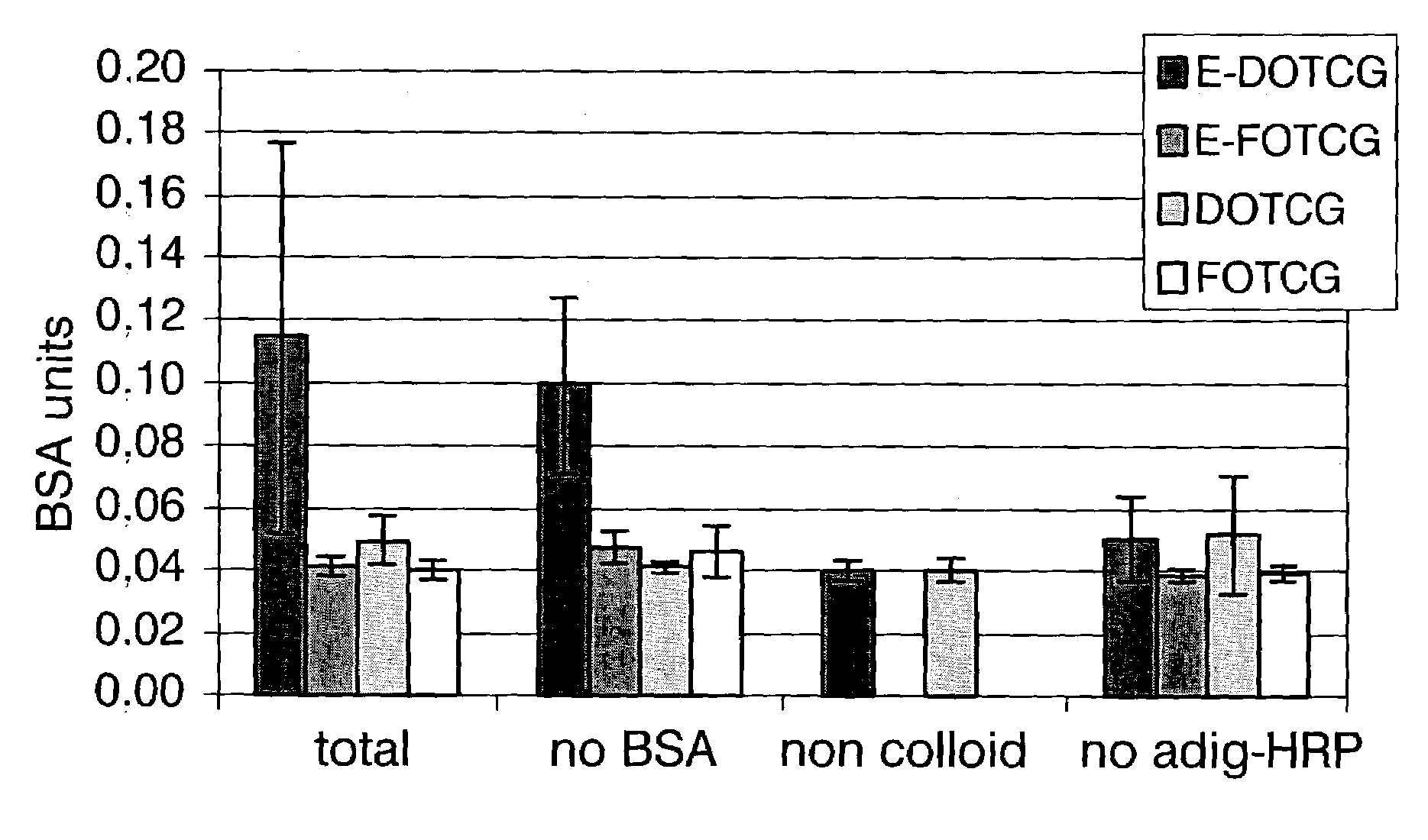
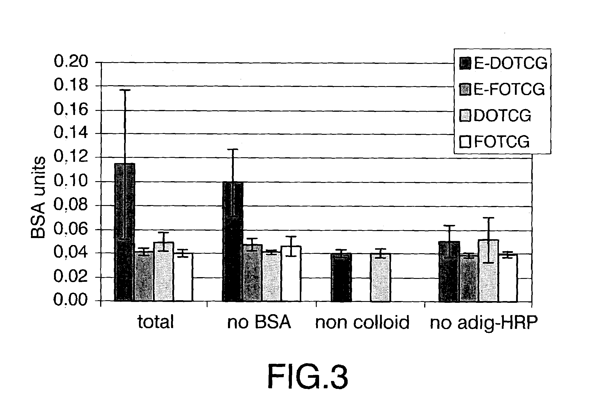
[0042]The DOTCG conjugates were prepared according to the process described by Storhoff and collaborators [Storhoff et al. (1998), Journal of the American Chemical Society, 120:1959–1964]. For this purpose, a colloidal gold commercial solution was added (CG) [Sigma, reference: G-1652 (gold colloid, 20 nm)] to a DOT solution and was mixed, in such a way that the final concentrations in the DOTCG conjugate were 2,54×10¹² particles mL−1 of colloidal gold of 20 nm and 3 μM of DOT. The mixture was left to react for 24 hours at room temperature and in the dark. Immediately after, the mixture was centrifuged at 5.000 rpm and 4° C. for 90 minutes. The supernatant was removed and the solid was redissolved in histidine buffer 50 mM, pH 7.5 (first wash). It was centrifuged for the second time under the same conditions, the supernatant was removed and the soli...


PUM


Abstract

A method includes (a) putting a multielectrodic chip lithographed in a wafer that contains between 2 and 2000 individually polarisable electrodes, in contact with a solution or suspension that includes modified colloidal particles with a (bio)chemical recognition element; (b) applying to an electrode of the multielectrodic chip, a potential between −1 and +2V vs. Ag / AgCl saturated, for a period of time between 1 and 300 seconds; (c) washing the chip after this stage (b); and (d) repeat the steps (b) and (c) as many times as needed to deposit a (bio)chemical recognition element, same or different to the one or ones previously deposited, on each one of the electrodes of that chip. The method is applicable for the fabrication of multisensors, particularly in chips and arrays for analytical and diagnostic applications.

Description

FIELD OF INVENTION[0001]In general, the invention relates to the deposition of an element and a chemical or biochemical recognition module on a substrate and, in particular, with a method to elaborate chips, multisensors, and arrays for clinical, environmental and food analysis or, for toxicity assays, identification of compounds in combinatorial processes and other applications in which multiple and fast analysis is necessary.BACKGROUND OF THE INVENTION[0002]In the last few years, great advances have been made in the development of chips (microelectronic devices) capable to characterise and identify analytes of interest. In general, a chip or multisensor for the detection of analytes is composed of a substrate over which is placed a plurality of individually addressable analysis sites (IAASs). Each IAAS includes a selectively immobilised specific receptor. This receptor can be of biological nature, for instance, antibody, enzyme, oligonucleotide, etc., or a living biological system...

Claims


Application Information

Patent Timeline
IPC IPC(8): H01L21/00B01J19/00C40B40/06G01N33/543
CPCB01J19/0046G01N33/54393B01J2219/00527B01J2219/00529B01J2219/00648B01J2219/00653B01J2219/00722C40B40/06
Inventor KATAKIS, IOANNISHOMS, MONICA CAMPAS
Owner UNIV ROVIRA I VIRGILI
Learn More