Eureka AIR delivers breakthrough ideas for toughest innovation challenges, trusted by R&D personnel around the world.

Two-dimensional photonic crystal, and waveguide and resonator using the same

a waveguide and waveguide technology, applied in waveguide type devices, instruments, cladded optical fibres, etc., can solve the problems of difficult production, difficult preparation of photonic crystals, and inability to maintain three-dimensional periodical structure, etc., and achieve the effect of easy preparation

Active Publication Date: 2006-11-14
TDK CORPARATION
View PDF23 Cites 6 Cited by
  • Summary
  • Abstract
  • Description
  • Claims
  • Application Information

AI Technical Summary

Benefits of technology

[0015]The present invention is to solve the aforementioned difficulties, and an object thereof is to provide a two-dimensional photonic crystal which is easy to prepare and has a complete band gap to the TE wave and the TM wave in all the incident angles, and a waveguide and a resonator utilizing the same.
[0017]Still another object of the invention is to increase the strength of the two-dimensional photonic crystal itself by utilizing a dielectric material other than air, thereby providing a two-dimensional photonic crystal that can be prepared easily. Also the invention, by utilizing a dielectric material other than air, enables to form a wider complete band gap and to achieve a relatively small size of a device utilizing the two-dimensional photonic crystal. Also the invention is to provide a two-dimensional photonic crystal capable of easily opening a band gap and reducing the loss by employing a ceramic material of a high relative dielectric constant, and a waveguide and a resonator utilizing the same.

Problems solved by technology

Such crystals have a wide complete band gap, but are very difficult to produce because of structures thereof Also in case one of the plural dielectric substances constituting the photonic crystal is air, the three-dimensional periodical structure cannot be maintained when the dielectric substances are arranged three-dimensionally and in a non-contact manner as in a certain diamond or opal structure.
Therefore, a thickness between the circular holes becomes as small as 0.04a, and such photonic crystal is very difficult to prepare.
Therefore, a complete band gap cannot be obtained in the two-dimensional photonic crystals constituted by such tetragonal lattices.
On the other hand, as the photonic crystal is generally prepared by a semiconductor manufacturing technology and a photoforming technology, materials to be employed are limited to semiconductor materials and photosettable resins.
These materials have relatively small relative dielectric constants, so that a wide band gap is difficult to obtain.
A method of mixing a ceramic powder in a photosettable resin is also known, but a high relative dielectric constant cannot be obtained as the relative dielectric constant is governed by a logarithmic mixing rule and is principally influenced by the relative dielectric constant of the resin, so that a wide band gap is difficult to obtain.

Method used


Image

  • Two-dimensional photonic crystal, and waveguide and resonator using the same
  • Two-dimensional photonic crystal, and waveguide and resonator using the same
  • Two-dimensional photonic crystal, and waveguide and resonator using the same

Examples


examples

[0057]In the following, the photonic crystal of the present embodiment will be explained by specific examples.

first example

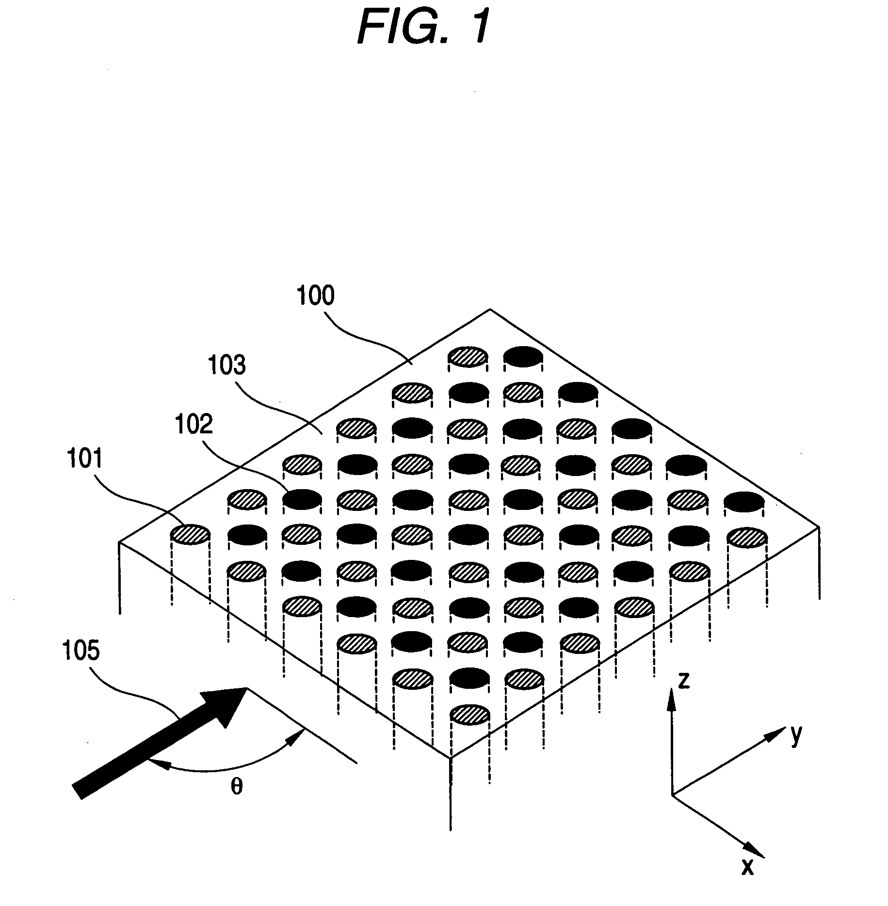
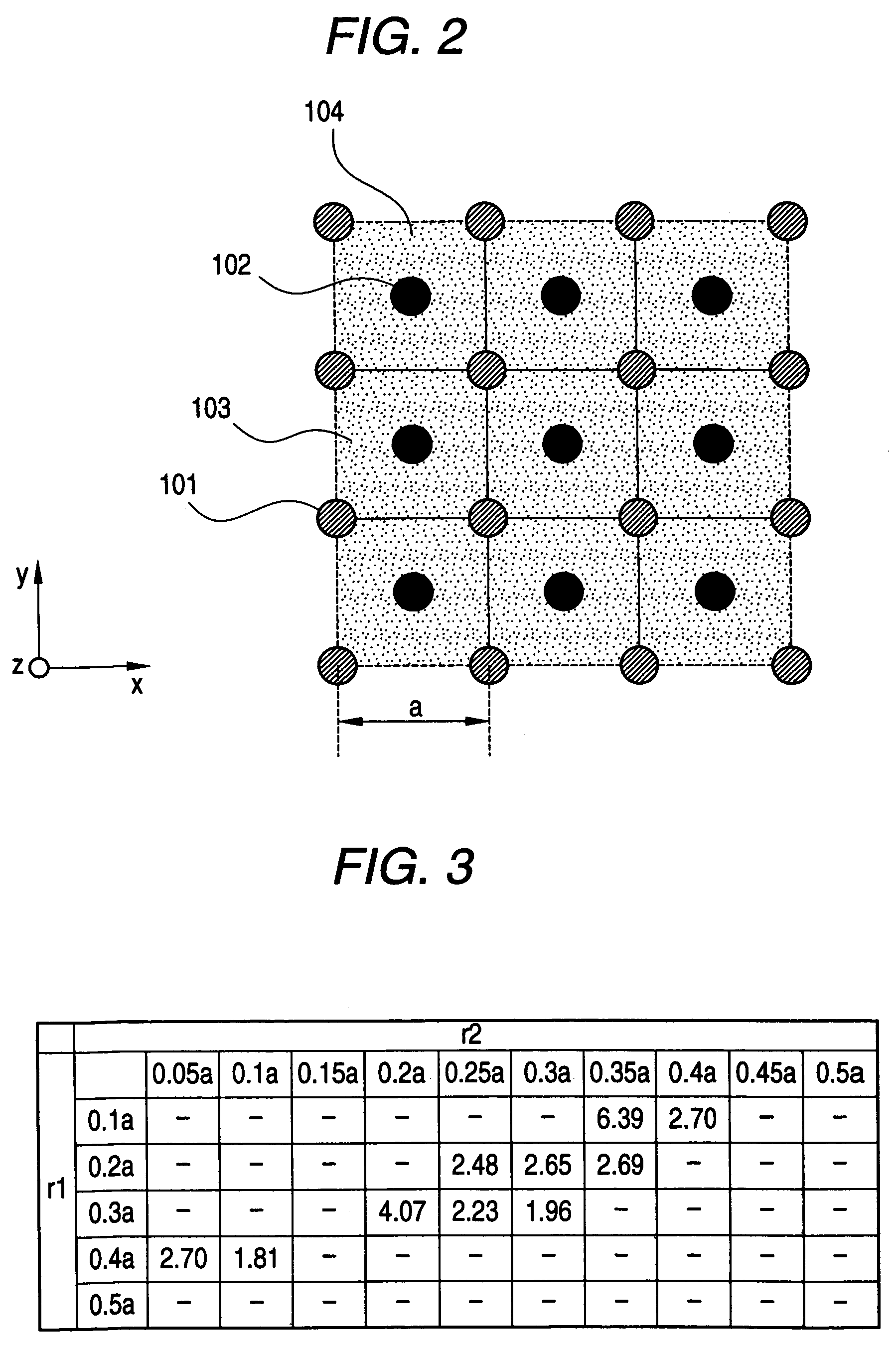
[0058]At first there will be explained a first example. In a photonic crystal 100 in the first example, a portion where the first cylindrical structural member 101 exists as the first dielectric area and a portion where the second cylindrical structural member 102 exists as the second dielectric area are vacant and are constituted by air. Therefore the first cylindrical structural member 101 and the second cylindrical structural member 102 have relative dielectric constants ∈1=∈2=1.0. Also the third dielectric area 103 is constituted of a material having a relative dielectric constant ∈3 of 10.4.

[0059]In the first example, a width of the complete band gap was calculated by a simulation conducted by varying the radius r1 of the first cylindrical structural member 101 and the radium r2 of the second cylindrical structural member 102. More specifically, the simulation was conducted by changing the cylindrical radius r1 and the cylindrical radius r2 respectively within a range of 0.1a t...

second example

[0064]In the following, there will be explained a second example. In a photonic crystal 100 in the second example, the first cylindrical structural member 101 constituting a first dielectric area is constituted of a material having a relative dielectric constant ∈1=10, while the second cylindrical structural member 102 has a radius r2 same as a radius r1 of the first cylindrical structural member 101. Also the third dielectric area 103 is vacant and is constituted by air. Therefore the third dielectric area 103 has a relative dielectric constant ∈3=1.0.

[0065]In the second example, a width of the complete band gap was calculated by a simulation conducted by varying the radius r1 of the first cylindrical structural member 101 and the radium r2 of the second cylindrical structural member 102. More specifically, the simulation was conducted by changing the cylindrical radius r1 (=cylindrical radius r2) within a range of 0.2 a to 0.3 a and by changing the relative dielectric constant ∈2 ...


PUM


Abstract

A tetragonal lattice is formed by first cylindrical structural members, and a photonic crystal has a periodical structure formed by a periodical arrangement of such tetragonal lattice. A distance between center points of the first cylindrical structural members is taken as a unit length a, which constitutes a lattice constant of the tetragonal lattice. At an approximate center of the tetragonal lattice, a cylindrical structural member is provided, and a dielectric area is provided around the first cylindrical structural members and the second cylindrical structural member. This structure allows the formation of a photonic band gap for a TE wave and a photonic band gap for a TM wave in a certain common frequency region, thereby forming a complete band gap.

Description

TECHNICAL FIELD [0001]The present invention relates to a photonic crystal adapted for use in a device for controlling an electromagnetic wave such as light, and more particularly to a two-dimensional photonic crystal capable of forming a complete photonic band gap to an electromagnetic wave of a specified wavelength region, and a waveguide and a resonator utilizing the same.BACKGROUND ART [0002]Recently, photonic crystals are becoming increasingly important as devices for controlling electromagnetic waves such as light. A photonic crystal is a periodical structured member showing a periodical change in a dielectric constant in crystal-constituting regions, with a periodical dielectric change comparable to a wavelength of an electromagnetic wave such as light, and can realize novel electromagnetic characteristics by an artificial periodical structure. Such structure is featured, like a band gap formation in a semiconductor substance by a Bragg reflection of electrons by periodical po...

Claims


Application Information

Patent Timeline
Patent Type & Authority Patents(United States)
IPC IPC(8): G02B6/10G02B6/02G02B6/122
CPCB82Y20/00G02B6/1225H01P1/2005G02B1/005G02B2006/12114
Inventor ENOKIDO, YASUSHI
Owner TDK CORPARATION
Why Eureka
Eureka Blog
Learn More