
Rotation-magnetron-in-magnetron (RMIM) electrode, method of manufacturing the RMIM electrode, and sputtering apparatus including the RMIM electrode

a technology of rmim and rmim, which is applied in the direction of electrolysis components, vacuum evaporation coatings, coatings, etc., can solve the problems of affecting the efficiency of rmim, so as to enhance step coverage and thickness uniformity and reduce the line width

Inactive Publication Date: 2006-10-10
SAMSUNG ELECTRONICS CO LTD
View PDF15 Cites 11 Cited by
  • Summary
  • Abstract
  • Description
  • Claims
  • Application Information

AI Technical Summary

Benefits of technology

The present invention provides a sputtering apparatus and a method for manufacturing it that can improve the plasma environment in a magnetron sputtering method for semiconductor device techniques. The apparatus includes a cylinder-shaped magnet and a plurality of ring-shaped magnets surrounding it, with the magnets having opposite magnetization directions. The driver unit supports and off-axis-rotates the magnet unit, and the plurality of ring-shaped magnets can even out the horizontal magnetic field distribution. The apparatus can provide a higher integration density and lower line width for semiconductor device techniques, as well as better step coverage and thickness for target etching.

Problems solved by technology

Use of a radio frequency (RF) or direct current (DC) bipolar sputtering method is simple, however, it takes a relatively long time to form layers, and during the formation of the layers, an increase in temperature, damage to layers, or component separation may occur.
In the magnetron sputtering method, however, it is very difficult to effectively control the movement of charged particles, particularly secondary electrons in a reactor, which is a critical factor affecting the performance of the magnetron sputtering method.
In addition, it is very difficult for the conventional magnetron sputtering apparatus adopting a magnetron cathode to meet the increasing needs of manufacturing highly integrated devices having a lower line width and processing larger-sized wafers.
These conventional magnetron cathode techniques have proven to be ineffective in processes for a low line width (0.14 μm or below) and a high aspect ratio (5:1 or greater) because they cause asymmetrically deposited thin films, deteriorating film uniformity, and ineffective use of target material accompanied by regionally etching of a target.

Method used


Image

  • Rotation-magnetron-in-magnetron (RMIM) electrode, method of manufacturing the RMIM electrode, and sputtering apparatus including the RMIM electrode
  • Rotation-magnetron-in-magnetron (RMIM) electrode, method of manufacturing the RMIM electrode, and sputtering apparatus including the RMIM electrode
  • Rotation-magnetron-in-magnetron (RMIM) electrode, method of manufacturing the RMIM electrode, and sputtering apparatus including the RMIM electrode

Examples


Embodiment Construction

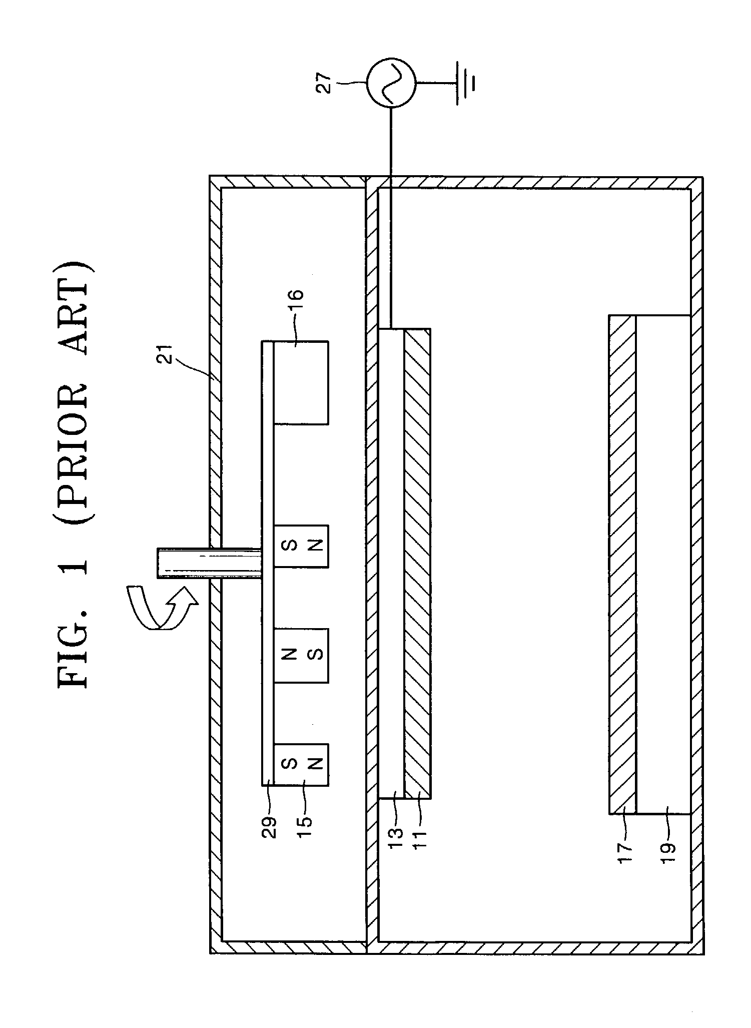
[0053]Korean Patent Application No. 2002-13938, filed Mar. 14, 2002, and entitled, “Rotation-Magnetron-in-Magnetron (RMIM) Electrode, Method of Manufacturing the RMIM Electrode, and Sputtering Aparatus Having the RMIM Electrode,” is incorporated by reference herein in its entirety.

[0054]Hereinafter, an RMIM electrode and a method for manufacturing the RMIM electrode according to the present invention will be described more fully with reference to the accompanying drawings in which preferred embodiments of the invention are shown. In the present invention, the RMIM electrode may be either an RMIM anode or an RMIM cathode. However, since an RMIM cathode is generally used in a sputtering apparatus, the RMIM electrode and the manufacturing method thereof according to the present invention will be described as an RMIM cathode and a manufacturing method thereof. Thus, it should be understood that the present invention may also be applied to an RMIM anode and a manufacturing method thereof...


PUM

PropertyMeasurementUnit
widthaaaaaaaaaa
diameteraaaaaaaaaa
diameteraaaaaaaaaa

Abstract

An RMIM electrode, a method for manufacturing the RMIM electrode, and a sputtering apparatus using the RMIM electrode, wherein the RMIM electrode includes a magnet unit including a cylinder-shaped magnet located at a center of the magnet unit and a plurality of ring-shaped magnets having increasingly larger diameters surrounding the cylinder-shaped magnet; and a driver unit for supporting and for off-axis-rotating the magnet unit, wherein in the magnet unit, adjacent magnets have opposite magnetization directions.

Description

BACKGROUND OF THE INVENTION[0001]1. Field of the Invention[0002]The present invention relates to a rotation-magnetron-in-magnetron (RMIM) electrode, a method of manufacturing the RMIM electrode, and a sputtering apparatus including the RMIM electrode. More particularly, the present invention relates to an RMIM electrode appropriate for a semiconductor device technique providing a high integration density and a low line width and a large-sized wafer process in a magnetron sputtering method, a method of manufacturing the RMIM electrode, and a sputtering apparatus having the RMIM electrode.[0003]2. Description of the Related Art[0004]Physical vapor deposition (PVD) and chemical vapor deposition (CVD) are generally used to manufacture thin films having a fine thickness. In a CVD method, a thin film having desired characteristics is obtained through chemical reactions. Alternately, in a PVD method, a thin film is formed by applying energy to a desired material so that the desired materia...

Claims


Application Information

Patent Timeline
Patent Type & Authority Patents(United States)
IPC IPC(8): H01J25/50H01J9/236C23C14/35H01J23/10H01J37/34H01L21/203
CPCC23C14/35H01J9/236H01J23/10H01J37/3408H01J37/3455
Inventor SHIN, JAI-KWANGKIM, SEONG-GUPARK, YOUNG-KYOUUM, HYEON-ILL
Owner SAMSUNG ELECTRONICS CO LTD
Learn More