
Ferroelectric capacitor devices and a method for compensating for damage to a capacitor caused by etching

a capacitor and device technology, applied in the field of ferroelectric capacitor devices and a method for compensating for capacitor damage caused by etching, can solve the problems of no replacement for the loss of other elements, detrimental to the characteristics of capacitors, and only partial compensation, so as to achieve the effect of compensating effectively for composition and crystallinity damag

Inactive Publication Date: 2006-10-10
POLARIS INNOVATIONS LTD
View PDF14 Cites 0 Cited by
  • Summary
  • Abstract
  • Description
  • Claims
  • Application Information

AI Technical Summary

Benefits of technology

"The present invention provides a method and device for compensating for damage to a capacitor caused by etching one or more exposed faces of a ferroelectric layer of the capacitor. The method includes depositing a seeding layer of ferroelectric material on the damaged faces, depositing a layer of material on the seeding layer, and applying an oxygen annealing recovery process to the capacitor. The device includes a substrate, electrodes, and an interlayer dielectric layer, with the ferroelectric layer formed between the electrodes and having one or more surfaces exposed by etching. The device also includes a seeding layer of ferroelectric material formed on the exposed surfaces of the ferroelectric layer and a further layer of material formed on the seeding layer. The technical effect of the invention is to effectively compensate for composition and crystallinity damage to the ferroelectric layer, improving the performance and reliability of the capacitor."

Problems solved by technology

Both of these defects are detrimental to the characteristics of the capacitor, and especially so for the vertical capacitor where the area exposed to the etching process is larger.
However, there is no replacement for the loss of other elements, such as lead, so the compensation is only partial.

Method used


Image

  • Ferroelectric capacitor devices and a method for compensating for damage to a capacitor caused by etching
  • Ferroelectric capacitor devices and a method for compensating for damage to a capacitor caused by etching

Examples


Embodiment Construction

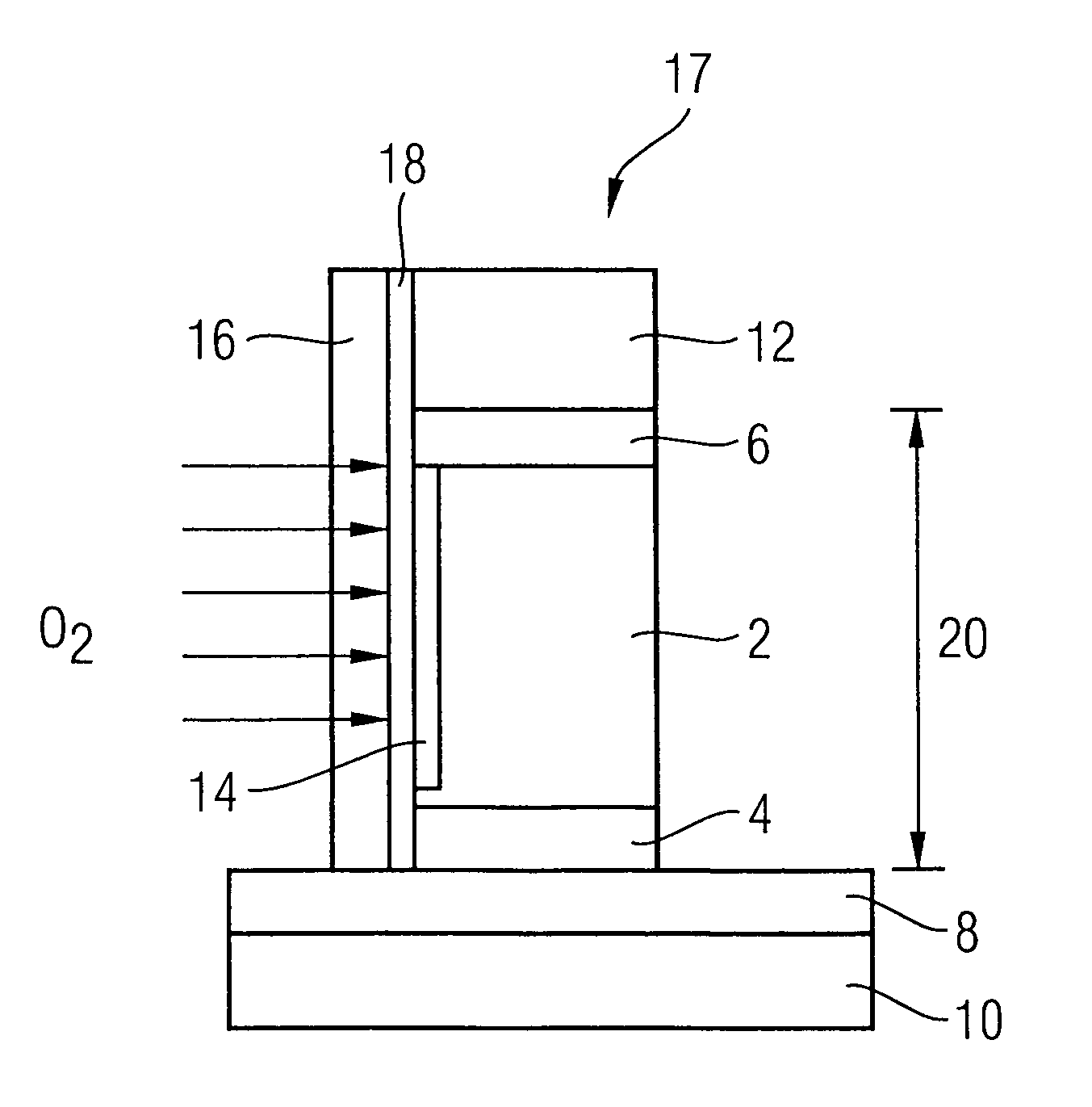
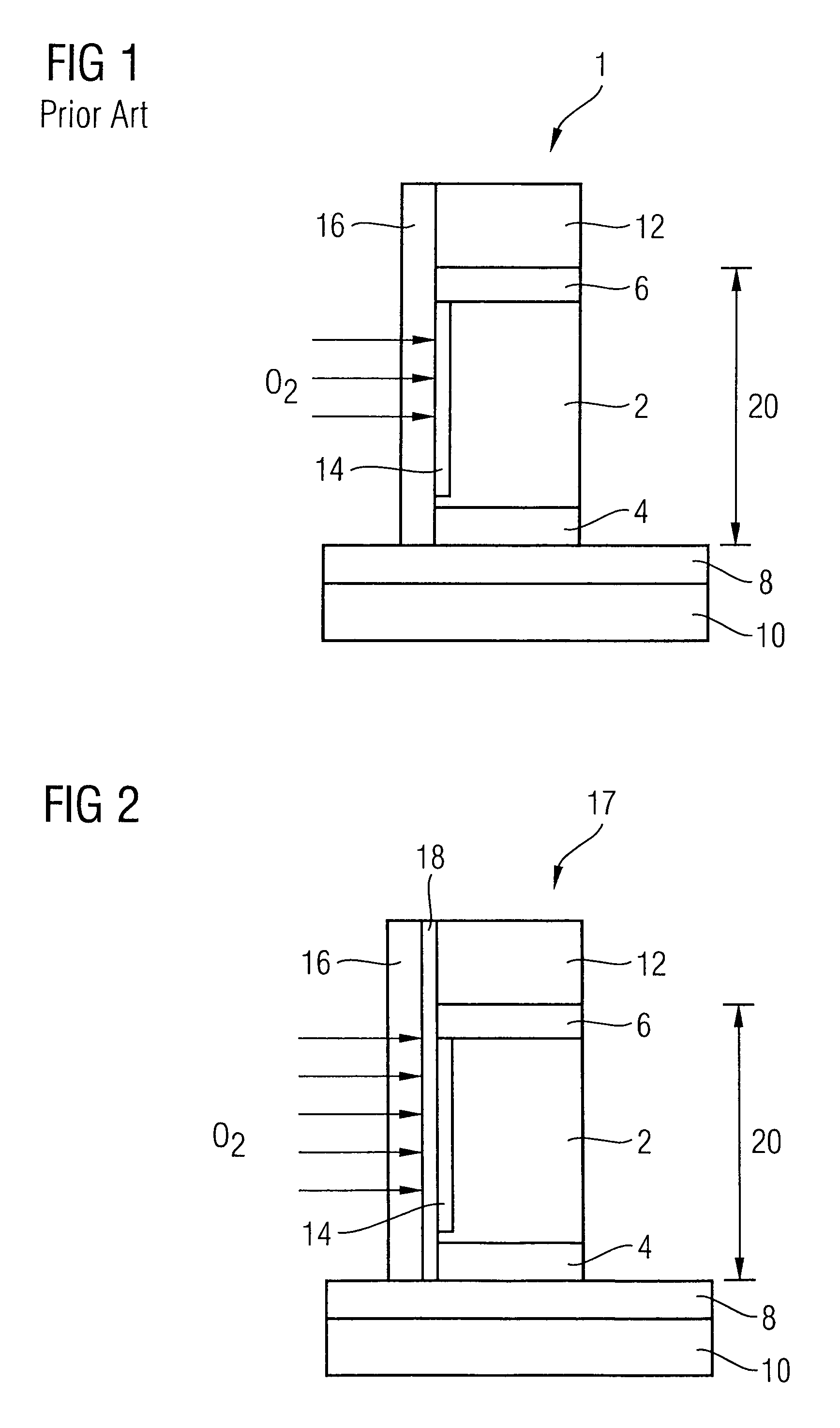
[0026]The method and device which illustrate an embodiment of the invention will be explained with reference to FIG. 2, The elements of the capacitor structure 17 illustrated in FIG. 2 which correspond exactly to elements in the capacitor 1 shown in FIG. 1 are allotted the same reference numerals.

[0027]In the embodiment shown in FIG. 2, a layer 18 of ferroelectric material, such as PZT, lead, or a combination of titanium and PZT, is deposited over the damaged wall faces 14 of the ferroelectric layer 2. This layer 18 of ferroelectric material acts as a seeding layer and may be deposited using, for example, a metal organic chemical vapour deposition (MOCVD) sputtering process. An electrode layer 16 formed of an electrically conductive material such as platinum is then deposited over the outer surface of this seeding layer 18.

[0028]The next stage in the process is recovery annealing in an oxygen atmosphere using RTA (rapid thermal annealing techniques) or a furnace. In one embodiment, ...


PUM

PropertyMeasurementUnit
ferroelectricaaaaaaaaaa
conductiveaaaaaaaaaa
shapeaaaaaaaaaa

Abstract

A ferroelectric capacitor in which damage caused by etching exposed faces of a ferroelectric layer of the capacitor is compensated by depositing a seeding layer of ferroelectric material such as PZT on one or more exposed faces of the ferroelectric layer and depositing an electrode layer made of conductive material such as platinum on the seeding layer. An oxygen annealing recovery process is applied to the device. The seeding layer can transform the phase of the damaged surfaces from amorphous to crystalline during the recovery annealing process and, at the same time, provide the damaged surfaces of the ferroelectric layer with missing element(s), for example lead. The oxygen necessary for recovery of the damage may be obtained through the platinum layer from the oxygen atmosphere.

Description

FIELD OF THE INVENTION[0001]The present invention relates to ferroelectric capacitor devices such as FeRAM devices, and a method for compensating for damage to a capacitor caused by etching.BACKGROUND OF THE INVENTION[0002]In general terms, ferroelectric capacitors are comprised of a ferroelectric layer sandwiched between two electrodes. The ferroelectric layer may be comprised of, for example, PZT, SBT or BLT. For horizontal ferroelectric capacitors, the layers are stacked in a horizontal manner starting with a lower electrode at the bottom followed by the ferroelectric layer and an upper electrode at the top. On the other hand, for a vertical ferroelectric capacitor structure, the electrodes are arranged vertically with the ferroelectric layer between two vertical electrodes A cross-sectional view of a conventional vertical ferroelectric capacitor is illustrated in FIG. 1. The vertical ferroelectric capacitor 1 includes a stack 20 comprised of a ferroelectric layer 2 sandwiched be...

Claims


Application Information

Patent Timeline
Patent Type & Authority Patents(United States)
IPC IPC(8): H01L21/302H01L21/02
CPCH01L28/56H01L28/75
Inventor MOON, BUM-KI
Owner POLARIS INNOVATIONS LTD
Learn More