Thin differential spin valve sensor having both pinned and self pinned structures for reduced difficulty in AFM layer polarity setting
a technology of differential spin valve and self-pinned structure, which is applied in the direction of magnetic recording, magnetic recording head, instruments, etc., can solve the problem that the setting process of 180° out-of-phase pinned structure becomes difficult for these types of sensors, and achieves the effect of higher read resolution
- Summary
- Abstract
- Description
- Claims
- Application Information
AI Technical Summary
Benefits of technology
Problems solved by technology
Method used
Image
Examples
first embodiment
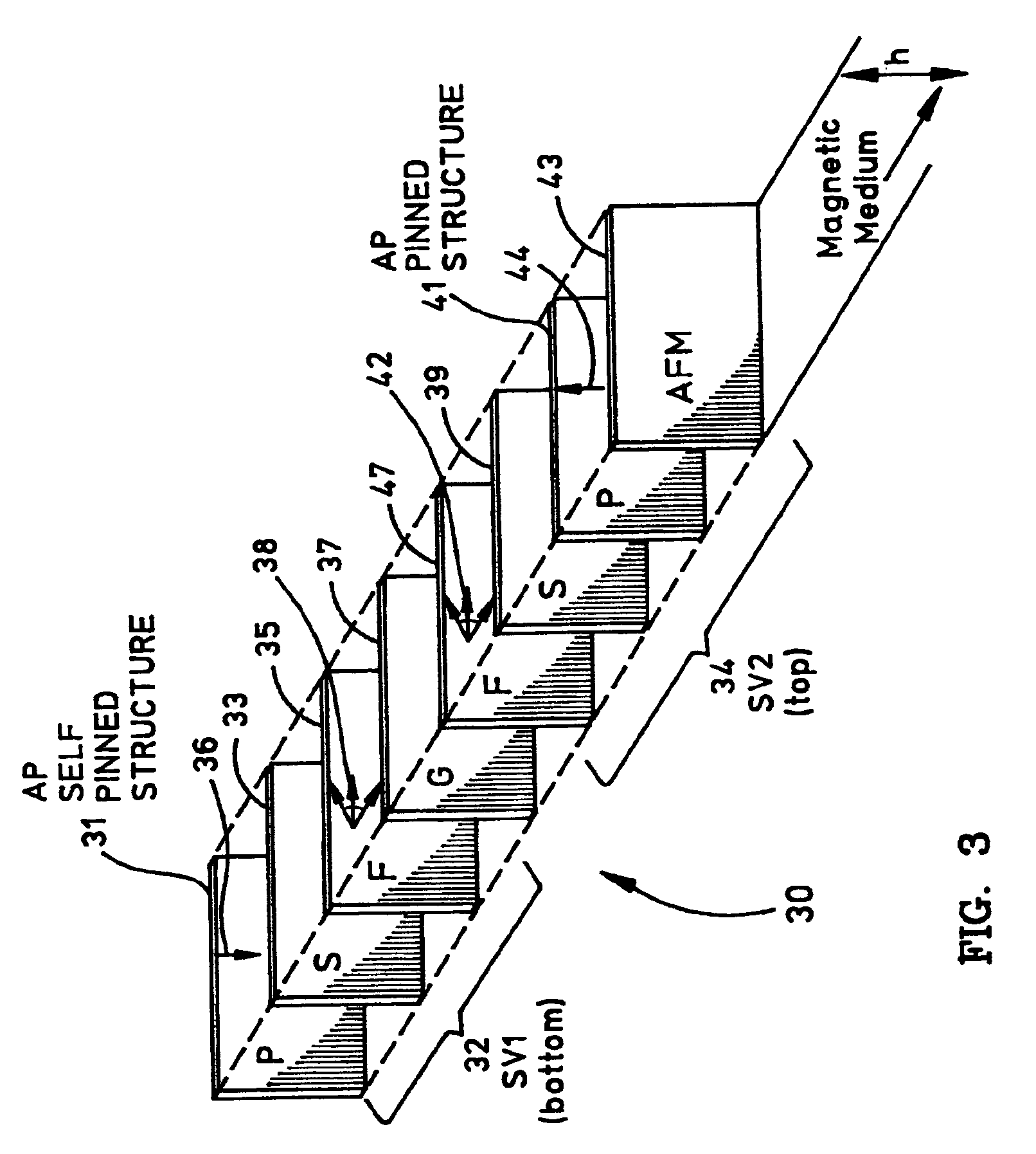
[0029]Referring now to FIG. 3, a dual / differential spin valve sensor 30 according to the present invention is shown. Sensor 30 includes first and second spin valve structures 32, 34 formed on a substrate and separated from each other by a thin layer of insulating gap material 37. Each spin valve structure 32, 34 has a first or “free” ferromagnetic (FM) layer 35, 47 separated by a thin nonmagnetic spacer layer 33, 39 from a second or “pinned” ferromagnetic (FM) layer 31, 41 in which the magnetization direction is fixed. Although not shown in detail in FIG. 3, each pinned layer 31 and 41 is actually a pinned layer structure which includes first and second FM layers with an antiparallel coupling (APC) layer sandwiched therebetween. A layer 43 of antiferromagnetic (AFM) material is deposited adjacent and in contact with pinned layer structure 41 to fix (i.e. pin) the magnetization direction in the pinned layer by exchange coupling. On the other hand, pinned layer structure 31 has a magn...
second embodiment
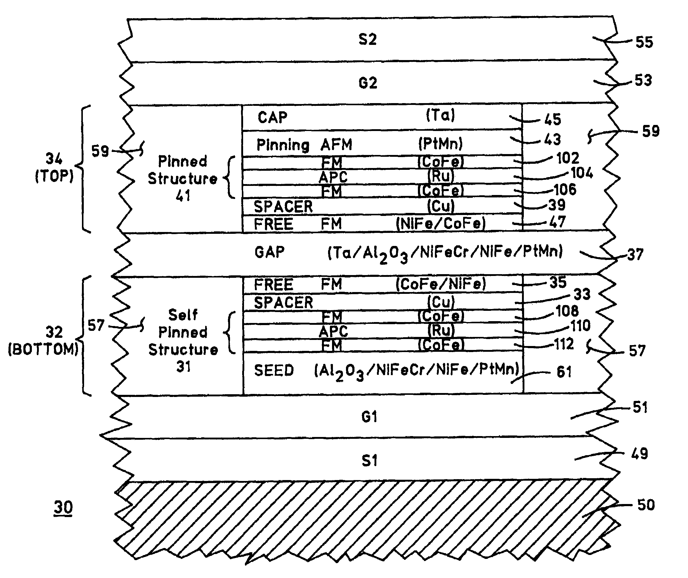
[0038]FIG. 5 is an ABS view of dual / differential spin valve sensor 30 in a Sensor 30 is similar to that shown and described in relation to FIGS. 3–4, except that pinned layer structure 41 (being exchanged-coupled) is provided in bottom spin valve structure 32 and pinned layer structure 31 (being self-pinned) is provided in top spin valve structure 34. Thus, pinning layer 43 is provided adjacent to pinned layer structure 41 (i.e. FM layer 106) over seed layer 61 in bottom structure 32, and no pinning layer is required in top structure 34. Seed layer 61 no longer needs the thin PtMn layer (compare seed layer 61 of FIG. 4) but may be formed simply as Al2O3 / NiFeCr / NiFe.
[0039]Dual / differential spin valve sensors are advantageous as they yield signals of opposite polarity under common mode excitation, thereby resulting in rejection of common mode noise and providing a higher read resolution determined by the gap layer which separates the two spin valve structures. Conventionally, the two...
PUM
| Property | Measurement | Unit |
|---|---|---|
| thick | aaaaa | aaaaa |
| thickness | aaaaa | aaaaa |
| non-magnetic electrically conductive | aaaaa | aaaaa |
Abstract
Description
Claims
Application Information
 - R&D
- Intellectual Property
- Life Sciences
- Materials
- Tech Scout
- Unparalleled Data Quality
- Higher Quality Content
- 60% Fewer Hallucinations
Browse by: Latest US Patents, China's latest patents, Technical Efficacy Thesaurus, Application Domain, Technology Topic, Popular Technical Reports.
© 2025 PatSnap. All rights reserved.Legal|Privacy policy|Modern Slavery Act Transparency Statement|Sitemap|About US| Contact US: help@patsnap.com


