Nitride semiconductor light-emitting device

a technology of semiconductor light-emitting devices and nitride semiconductors, which is applied in the direction of semiconductor devices, basic electric elements, electrical appliances, etc., can solve the problems of layer alone not being able to completely solve, the difference in the lattice constant, and the crystal defect of the crystal, so as to reduce the density of the compensation acceptor, improve crystallinity, and reduce the free electron concentration

Active Publication Date: 2006-10-03
SAMSUNG ELECTRONICS CO LTD
View PDF8 Cites 1 Cited by
  • Summary
  • Abstract
  • Description
  • Claims
  • Application Information

AI Technical Summary

Benefits of technology

[0011]Therefore, the present invention has been made in view of the above problems, and it is an object of the present invention to provide a nitride semiconductor light-emitting device having an active layer doped with a small amount of Al, a group III element of the periodic table, in order to reduce a carrier capture effect due to crystal defects and thus substantially increase an effective amount of carrier.
[0021]In accordance with the present invention, a small amount of Al incorporation into the active layer decreases the density of the compensation acceptors by the substitution of Al atoms for Ga vacancy sites. It is well known that a Ga vacancy has a deep acceptor state and thus acts as a compensating center, which decreases the free electron concentration in an n-type GaN material. Thus, the active layer doped with a small amount of Al has improved crystallinity and also increased concentration of carrier.

Problems solved by technology

However, there in no commercially available substrate having the same crystal structure as that of the nitride semiconductor while exhibiting lattice matching therebetween, and thus a sapphire substrate, which is electrically insulative, is primarily used.
Consequently, there are crystal defects resulting from difference in a lattice constant and thermal expansion coefficient between the sapphire substrate and the nitride semiconductor layer grown thereon.
In order to lower this problem, a buffer layer may be used on the sapphire substrate, but the buffer layer alone cannot completely resolve such a problem associated with crystal defects.
In particular, in InGaN / GaN layer used as an active layer for generating / emitting a blue-green light, these crystal defects raise a problem of greatly reducing a light-gain.
In particular, where the active layer has a multiple quantum well structure, the layer is relatively thicker compared to a single quantum well structure, thereby increasing series resistance, in turn increasing a driving voltage and therefore has significantly deteriorated electrical and optical characteristics thus requiring higher doping concentration.
As described above, the scheme of Si or Ge doping necessarily requires an excessive amount of impurities doping, in order to effectively increase the light-gain and thus may present a factor causing crystallinity deterioration.
Further, due to a band-tail phenomenon, an oscillating light shifts to a long wavelength region and thus it is difficult to design a light-emitting device with a desired short wavelength.

Method used


Image

  • Nitride semiconductor light-emitting device
  • Nitride semiconductor light-emitting device
  • Nitride semiconductor light-emitting device

Examples


Embodiment Construction

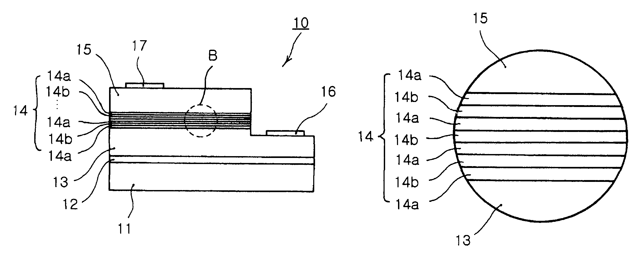
[0028]Now, the present invention will be described in detail with reference to the attached drawings. FIG. 1a shows a structure of a nitride semiconductor light-emitting device in accordance with the present invention.

[0029]Referring to FIG. 1a, a nitride semiconductor light-emitting device 10 includes a first nitride semiconductor layer 13, an active layer 14 and a second nitride semiconductor layer 15, sequentially formed on a sapphire substrate 11. A buffer layer 12 may be further formed on the sapphire substrate 11 to provide for lattice matching therebetween. Further, a first electrode 16 is formed on the upper surface of the mesa etched first nitride semiconductor layer 13 while a second electrode 17 is formed on the upper surface of the second nitride semiconductor layer 15.

[0030]The active layer 14 is composed of a quantum barrier layer 14a of material having the formula of Inx1Ga1−x1N wherein x1 is a number between 0 and 1, and a quantum well layer 14b of material having th...


PUM


Abstract

A nitride semiconductor light-emitting device includes a first conductive nitride semiconductor layer; an active layer formed on the first conductive nitride semiconductor layer, and having at least one quantum well layer and at least one quantum barrier layer alternatively laminated; and a second conductive nitride semiconductor layer formed on the active layer, wherein at least one of the quantum well layer and quantum barrier layer in the active layer is doped with elemental Al in a concentration of less than 1%.

Description

RELATED APPLICATIONS[0001]The present application is based on, and claims priority from, Korean Application Serial Number 2004-39101, filed May 31, 2004, the disclosure of which is hereby incorporated by reference herein in its entirety.BACKGROUND OF THE INVENTION[0002]1. Field of the Invention[0003]The present invention relates to a nitride semiconductor light-emitting device, and more particularly to a nitride semiconductor light-emitting device having improved electrical and optical characteristics by improving crystallinity of an active layer.[0004]2. Description of the Related Art[0005]Recently, advent of a nitride semiconductor capable of emitting a blue-green light has lead to realization of three primary colors and white light in semiconductor light-emitting devices. Therefore, application areas of light-emitting devices made of such a nitride semiconductor are further extended and thus widely used in lightings in which high-directivity is required, such as back light source...

Claims


Application Information

Patent Timeline
Patent Type & Authority Patents(United States)
IPC IPC(8): H01L33/00H01L33/06H01L33/32
CPCH01L33/32H01L33/06
Inventor LEE, JAE HOONKIM, YONG CHUNKIM, JE WON
Owner SAMSUNG ELECTRONICS CO LTD
Why Eureka
Try Eureka