Method for precisely forming light emitting layers in a semiconductor device

Inactive Publication Date: 2006-10-03
SEMICON ENERGY LAB CO LTD
View PDF125 Cites 32 Cited by
  • Summary
  • Abstract
  • Description
  • Claims
  • Application Information

AI Technical Summary

Benefits of technology

[0015]In the thin film forming apparatus of FIGS. 1A and 1B, the head portion 106 is fixed, and the transport stage 101 on which the substrate 102 is put is moved in the X-direction or Y-direction. That is, such a mechanism is adopted that the transport stage is moved so that the head portion 106 is relatively moved over the substrate 102. Of course, although it is also possible to make such a mechanism that the head portion 106 is moved, the stability is superior when the substrate side is moved.
[0027]Note that the bank 121 made of a resin material is provided between pixels, and prevents the coating liquids from being mixed between adjacent pixels. In this structure, when the width (determined by the resolution of photolithography) of the bank 121 is made narrow, the integration of the pixel portion is improved and an image of high fineness can be obtained. Particularly, in the case where the viscosity of the coating liquid is 1 to 30 cp, it is effective.

Problems solved by technology

However, in the ink-jet method, since the high molecular EL material is jetted and is scattered, if a distance between a coated surface and a nozzle of a head for ink jet is not made suitable, there can occur a problem of a so-called flying curve in which a droplet falls to a portion other than a necessary portion.

Method used


Image

  • Method for precisely forming light emitting layers in a semiconductor device
  • Method for precisely forming light emitting layers in a semiconductor device
  • Method for precisely forming light emitting layers in a semiconductor device

Examples


embodiment 1

[Embodiment 1]

[0055]In the mode of carrying out the invention, the description has been made on the example in which three kinds of stripe-shaped luminescent layers emitting lights of red, green and blue are formed in the vertical or horizontal direction at the same time. In this embodiment, a description will be made on an example in which a stripe-shaped luminescent layer is divided into plural portions in the longitudinal direction and is formed.

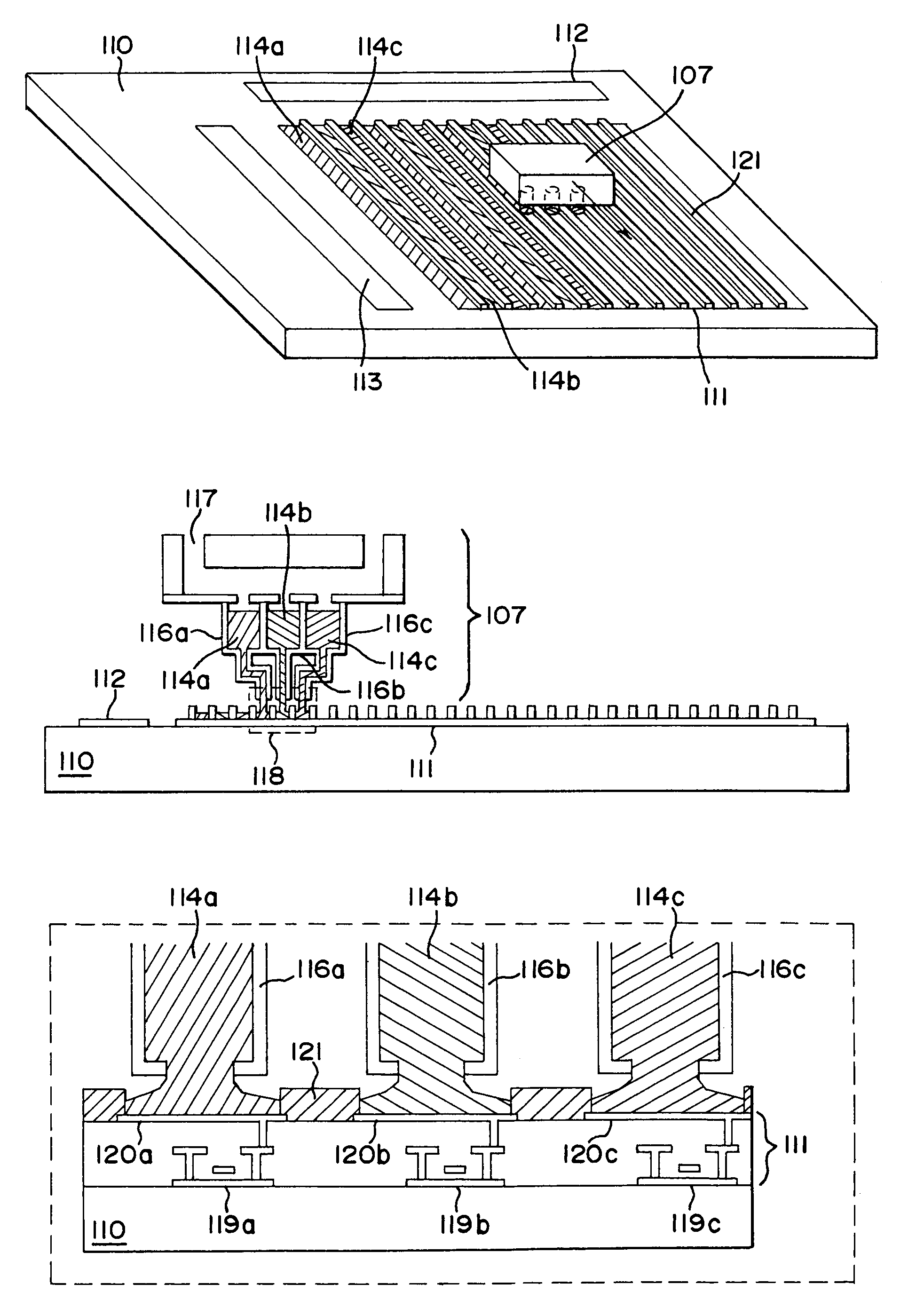
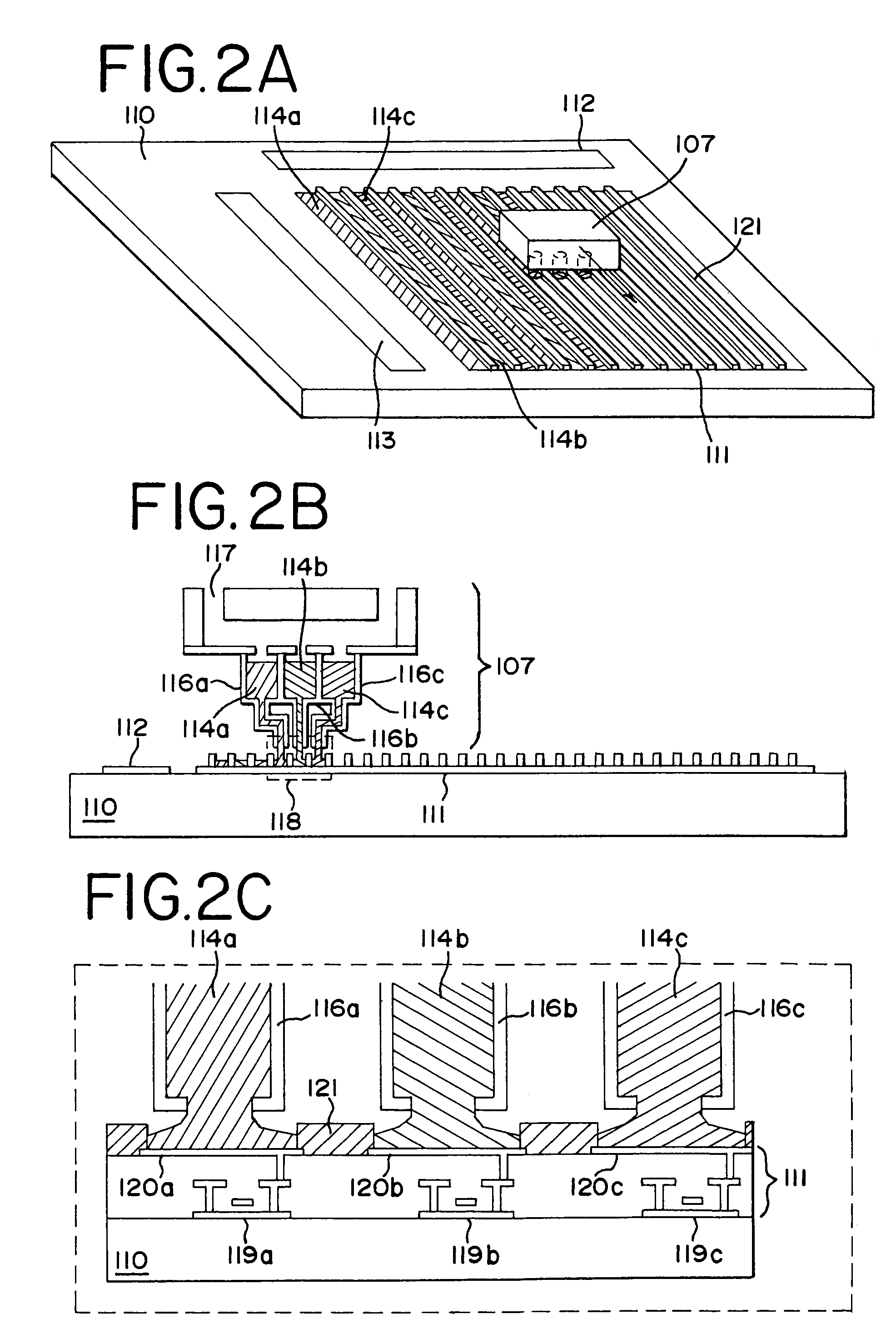
[0056]As shown in FIG. 3A, a pixel portion 111, a source side driving circuit 112, and a gate side driving circuit 113 comprises TFTs on a substrate 110, and the pixel portion 111 is divided into matrix form by banks 301. In the case of this embodiment, in one square 302 separated by the banks 301, as shown in FIG. 3B, a plurality of pixels 303 are disposed. The number of pixels is not limited.

[0057]In such a state, a film formation step of an organic EL material functioning as a luminescent layer is carried out by using the thin film for...

embodiment 2

[Embodiment 2]

[0062]When the direction of the pixel line shown in FIG. 2A is made the vertical direction, the bank 121 is formed along the source wiring line. Thus, it can be said that the pixel line in the case where the bank is formed along the gate wiring line is formed in the horizontal direction. That is, in the case where the pixel line is formed in the vertical direction, the arrangement becomes as shown in FIG. 4A, and in the case where the pixel line is formed in the horizontal direction, the arrangement becomes as shown in FIG. 4B.

[0063]In FIG. 4A, reference numeral 401 designates a bank formed into a stripe shape in the vertical direction: 402a, an EL layer emitting red light: and 402b, an EL layer emitting green light. Of course, an EL layer (not shown) emitting blue light is formed adjacent to the EL layer 402b emitting green light. Note that the bank 401 is formed over the source wiring line through an insulating film and along the source wiring line.

[0064]The EL layer...

embodiment 3

[Embodiment 3]

[0069]In this embodiment, a description will be made on an example of a case where the thin film forming apparatus of the present invention is incorporated in a thin film forming apparatus of a multi-chamber system (or also called a cluster tool system), and a forming process of an EL element is continuously carried out without opening to the air.

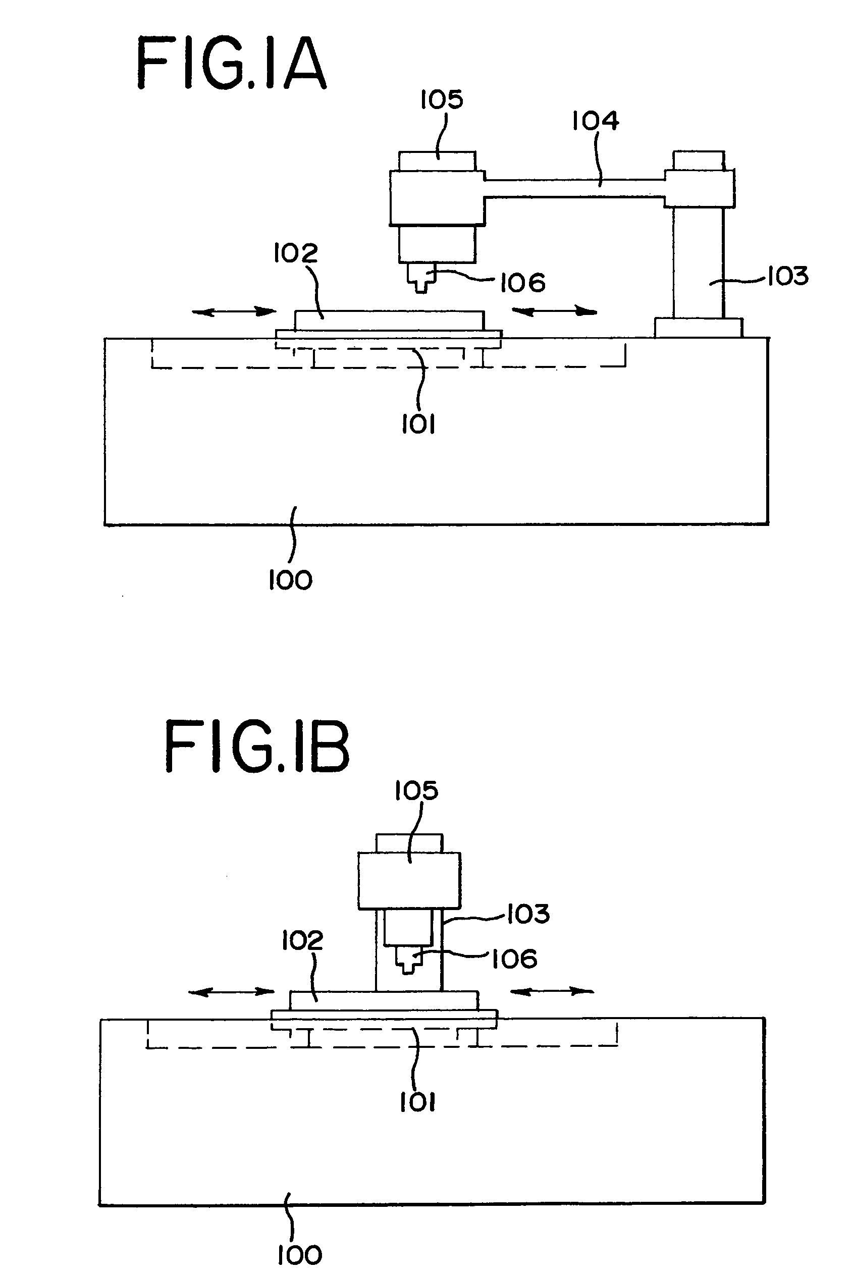
[0070]In FIG. 5, reference numeral 501 designates a common chamber, and the common chamber 501 is provided with a transporting mechanism (A) 502 by which a substrate 503 is transported. An atmosphere of the common chamber 501 is made reduced, and the common chamber 501 is shut off from respective treatment chambers by gates. The transfer of the substrate to the respective treatment chambers is carried out by the transporting mechanism (A) 502 when the gate is opened. In order to reduce the pressure of the common chamber 501, although it is possible to use an exhaust pump such as an oil rotation pump, a mechanical booster pump,...


PUM

PropertyMeasurementUnit
Coloraaaaaaaaaa
Luminescenceaaaaaaaaaa

Abstract

There is provided a method for precisely forming light emitting layers in a semiconductor device without a positional deviation and at a high throughput. A pixel portion is divided into a plurality of signal lines by banks, and a coating liquid (R), a coating liquid (G), and a coating liquid (B) are applied respectively in a stripe shape at the same time using a dispenser. Then, luminescent layers emitting lights of respective colors of red, green and blue can be formed by heating these coating liquids.

Description

[0001]This application is a divisional of U.S. application Ser. No. 09 / 685,912, filed on Oct. 10, 2000 now abandoned.BACKGROUND OF THE INVENTION[0002]1. Field of the Invention[0003]The present invention relates to a thin film forming apparatus used for fabricating an EL element having a structure in which a luminescent material capable of generating EL (Electro Luminescence), particularly, a luminescent organic material (hereinafter referred to as organic EL material) is placed between an anode and a cathode.[0004]2. Description of the Related Art[0005]In recent years, a display device which uses an EL element as a self-luminous element using an EL phenomenon of an organic EL material (EL display device) has been developed. Since the EL display device is of a self-luminous type, a backlight as in a liquid crystal display device is not necessary. Further, since an angle of visibility is wide, the EL display device is regarded as promising as a display portion of a portable equipment ...

Claims


Application Information

Patent Timeline
IPC IPC(8): H01L21/00H01L51/40H05B33/10H01L27/32H01L51/00H01L51/30H01L51/50H01L51/56H05B33/12
CPCH01L51/0004H01L51/0005H01L27/3211H01L27/3244H01L27/3295H01L51/0035H01L51/0038H01L51/0042H01L51/56H10K59/35H10K71/13H10K71/135H10K59/122H10K85/114H10K85/146H10K85/111H05B33/10H10K59/12H10K71/00
Inventor YAMAZAKI, SHUNPEIYAMAMOTO, KUNITAKAHIROKI, MASAAKIFUKUNAGA, TAKESHI
Owner SEMICON ENERGY LAB CO LTD
Why Eureka
Try Eureka