Dc/ac conversion device and ac power supply method
a conversion device and ac power supply technology, applied in the direction of electric variable regulation, process and machine control, instruments, etc., can solve the problems of low power inversion efficiency, inability to maintain a constant output voltage, and difficulty in miniaturizing such inverters, so as to reduce the effect of switching loss
- Summary
- Abstract
- Description
- Claims
- Application Information
AI Technical Summary
Benefits of technology
Problems solved by technology
Method used
Image
Examples
first embodiment
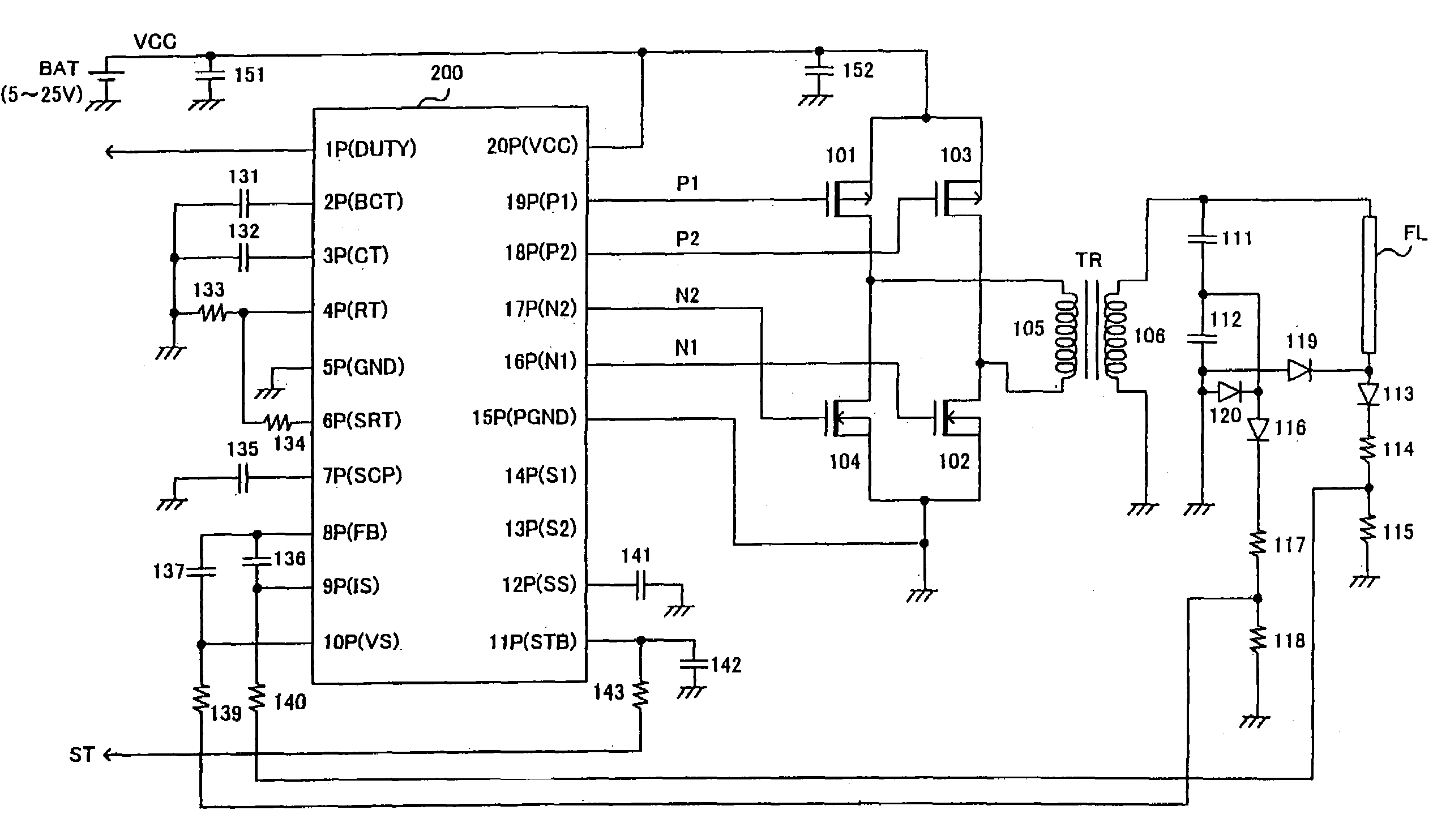
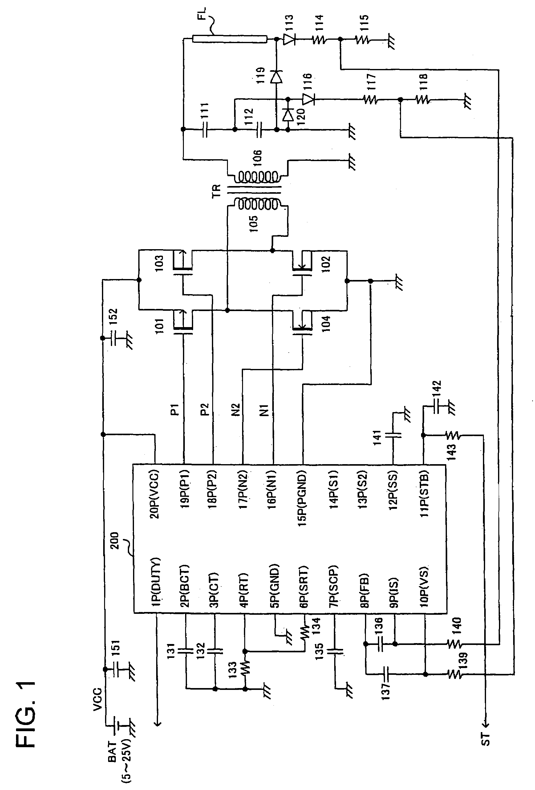
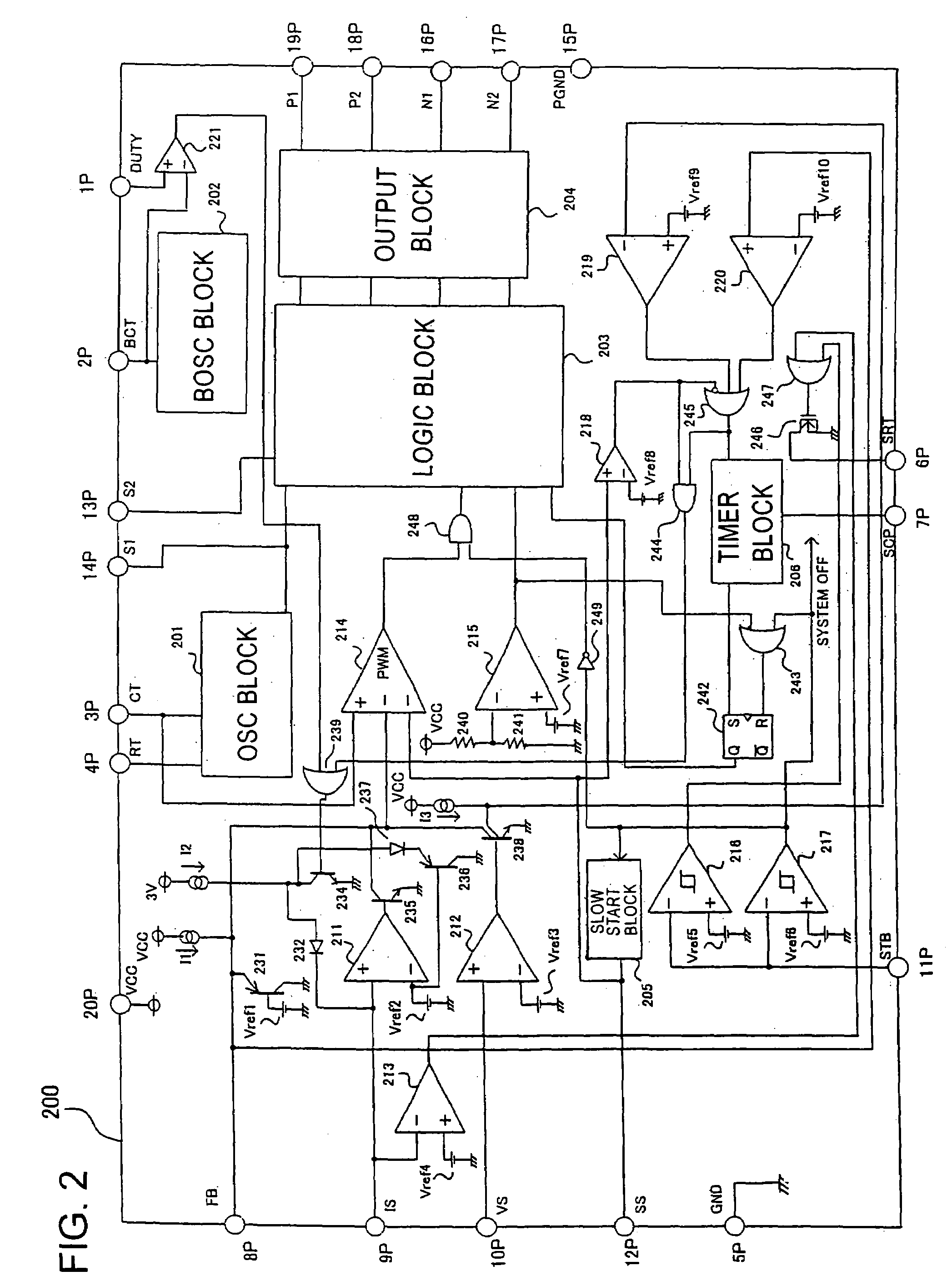
[0095]Referring to FIG. 1, there is shown an over-all arrangement of a first inverter according to the invention that utilizes an insulated transformer and a full-bridge switch circuit to carry out PWM control. FIG. 2 illustrates the internal structure of a controller IC (i.e. IC for controlling inverter) for use in the inverter of FIG. 1. FIG. 3 is a timing diagram for a FIG. 4 is a timing diagram illustrating further details of a part of the timing diagram shown in FIG. 3. FIG. 5 illustrates the operating conditions of the full-bridge at different stages the each timing.
[0096]As shown in FIG. 1, a first switch in the form of a P-type MOSFET (hereinafter referred to as PMOS) 101 and a second switch in the form of an N-type MOSFET (hereinafter referred to as NMOS) 102 constitute a current path in a first direction to the primary winding 105 of a transformer TR. A third switch in the form of a PMOS 103 and a fourth switch in the form of NMOS 104 constitutes a second current path in ...
second embodiment
[0167]The current in the first direction will become zero when the energy stored in the transformer TR1 is exhausted. Thus, a condition of zero current is also established in the second embodiment before the direction of the current through the primary winding 308 is switched.
[0168]Such zero-current condition prior to the switching of the current direction can be attained by optimizing the pulse width in the PWM control in accordance with electric properties of the transformer TR1, resonance capacitors 311, 312, 315 and 316, cold cathode fluorescent lights FL11 and FL12, etc. involved.
[0169]In the period iii when the gate drive signal P1 has gone to L level, a current flows in the second direction from the power supply BAT to the primary winding 308 via the PMOS 303 and the second capacitor 304.
[0170]In period iv when the gate drive signal P1 is H level, a simultaneous OFF period Toff is established in which both the PMOS 303 and NMOS 302 are turned off, thereby preventing a penetra...
PUM
 Abstract
Description
Claims
Application Information
 - R&D
- Intellectual Property
- Life Sciences
- Materials
- Tech Scout
- Unparalleled Data Quality
- Higher Quality Content
- 60% Fewer Hallucinations
Browse by: Latest US Patents, China's latest patents, Technical Efficacy Thesaurus, Application Domain, Technology Topic, Popular Technical Reports.
© 2025 PatSnap. All rights reserved.Legal|Privacy policy|Modern Slavery Act Transparency Statement|Sitemap|About US| Contact US: help@patsnap.com


