
Analog signal sampling system and method having reduced average input current

a sampling system and input current technology, applied in transmission systems, analogue/digital conversion, instruments, etc., can solve the problems of limiting the increase of conversion accuracy, sampling error, corresponding quadratic increase in input current, etc., and achieve the effect of reducing the average charge taken and greatly reducing the effect of input source resistance on measurement accuracy

Active Publication Date: 2006-08-08
ANALOG DEVICES INT UNLTD
View PDF15 Cites 6 Cited by
  • Summary
  • Abstract
  • Description
  • Claims
  • Application Information

AI Technical Summary

Benefits of technology

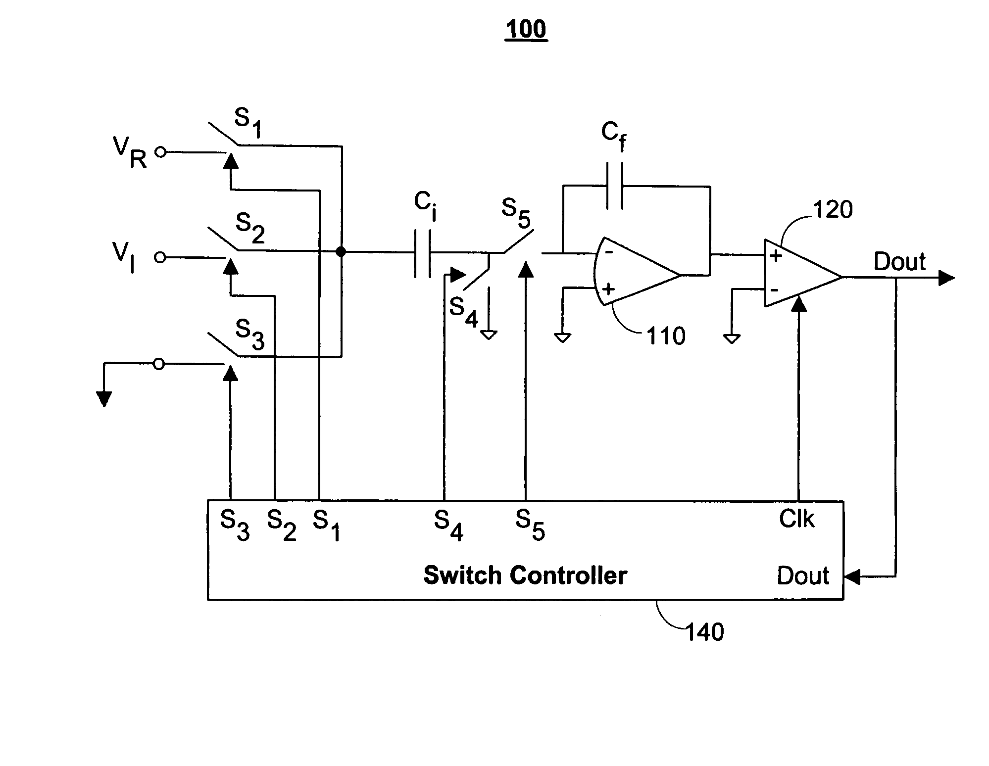
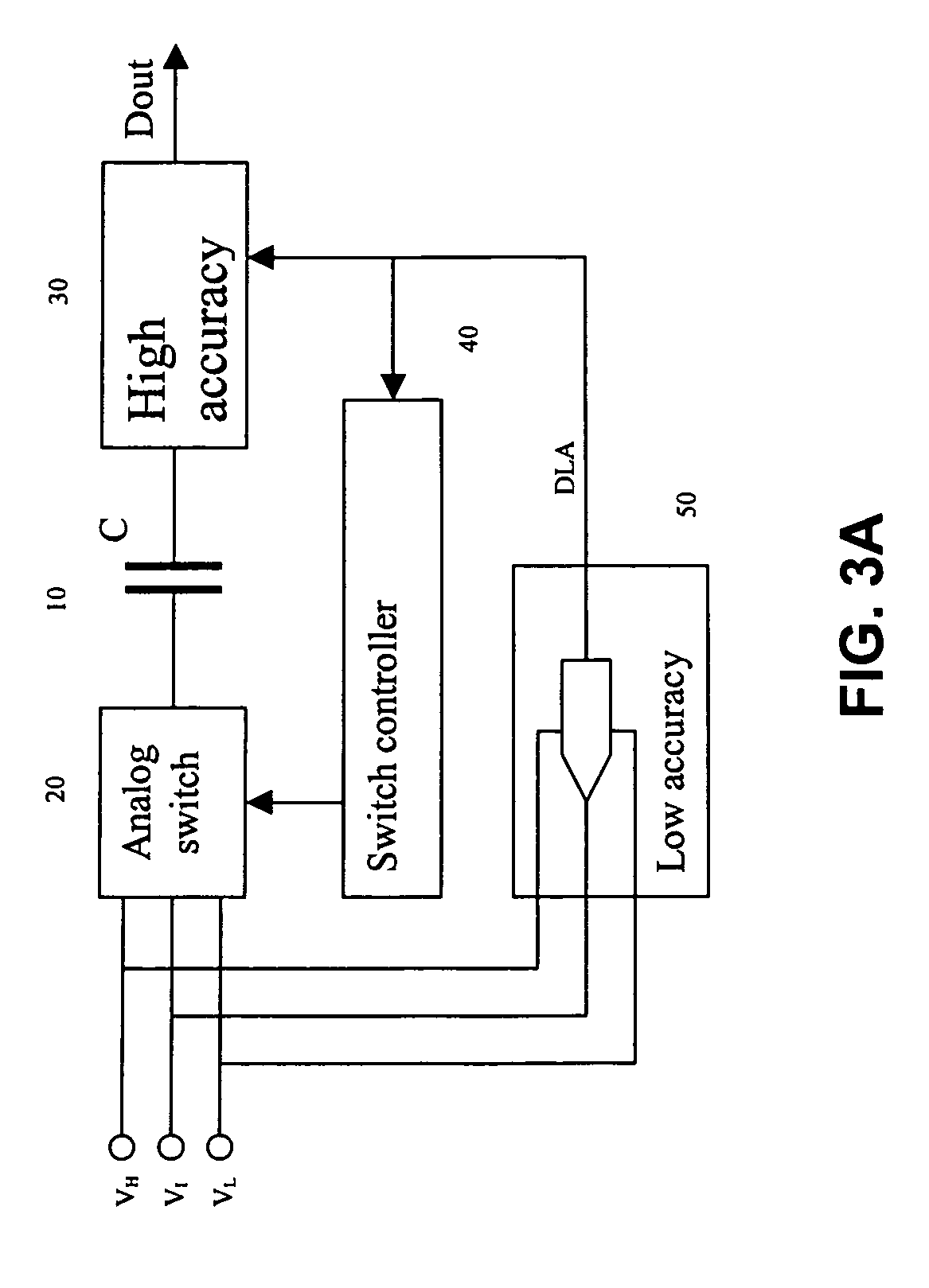
The present patent offers a novel signal sampling system and methodology that reduces the average charge taken from the input signal source without substantially altering the instantaneous charge transferred between the input signal source and a modulator. This is achieved by controlling the sampling device to provide a substantially zero total charge taken by the sampling device from the input signal source. The system includes a sampling device and a switching circuit that supplies the input signal and a reference signal to the sampling device. The switching circuit is controlled to provide a substantially zero total charge taken by the sampling device from the input signal source. The method involves determining the number of sample sequences in which the reference signal should be supplied and supplying the reference signal in these sequences. The system also includes a differential-in / d differential-out voltage amplifier for producing a differential output signal. The technical effects of this patent include reducing the average differential input current of the sampling circuit, minimizing the impact of input signal source resistance on measurement accuracy, and improving the accuracy of the measurement.

Problems solved by technology

On the other hand, recent developments in sensor technology, improvements in converter resolution and converter speed have made such errors quadratic factors limiting further increase in conversion accuracy.
As this input current passes through the signal source impedance, it causes a voltage change, modifying the original input value and creating a sampling error.
Due to thermal noise limitations, an increase in the conversion resolution requires a quadratic increase in the size of the sampling capacitors resulting in the corresponding quadratic increase in the input current.
This is a very difficult goal to achieve and it rapidly becomes impractical as the desired conversion accuracy and speed increase.
The source impedance of a sensor imposes a theoretical limit on available ranges of conversion speed and resolution.
Unavoidable parasitic capacitors and necessary signal filter capacitors involved in practical configurations further limit these ranges.
Configurations using external buffers offer great flexibility but place an unacceptable heavy burden upon the user in order to maintain the global accuracy of the measurement chain.
These configurations also demand supplemental power supply rails, critical power supply sequencing circuits and an additional physical space.
Nevertheless, the integrated buffers limit the analog-to-digital converter overall accuracy and dynamic range.

Method used


Image

  • Analog signal sampling system and method having reduced average input current
  • Analog signal sampling system and method having reduced average input current
  • Analog signal sampling system and method having reduced average input current

Examples


Embodiment Construction

[0036]The present disclosure will be made using the example of an over-sampling analog-to-digital (A / D) converter. It will become apparent, however, that the concepts described herein are applicable to any type of circuit that implements sampling of analog signals.

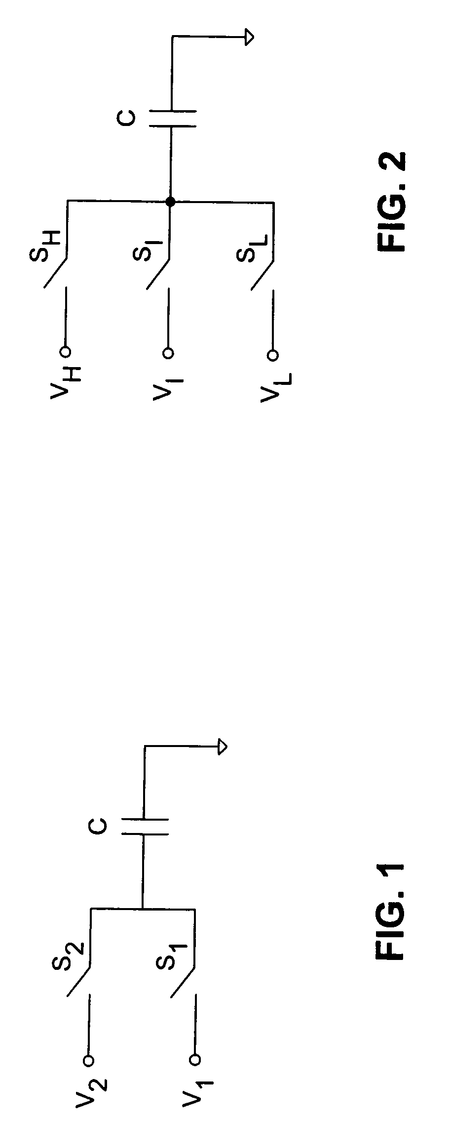
[0037]The instantaneous charge required from an input signal source in any single sampling operation is proportional to the size of the sampling capacitors as well as to the amount of charge stored in these capacitors prior to the sampling operation. For example, as shown in FIG. 1, one terminal of a sampling capacitor C is connected to a reference voltage, e.g., to ground. The second terminal may be supplied through a switch S1 with a voltage V1 or through a switch S2 with a voltage V2. The voltages V1 and V2 are defined with respect to the established ground level.

[0038]Assuming that initially the switch S1 is closed and the switch S2 is open the charge Q1 stored in the sampling capacitor C is:

Q1=V1*C.

[0039]In the second...


PUM


Abstract

A novel sampling system having a sampling device responsive to an analog input signal and a reference signal for providing corresponding charges. A switching circuit is provided to supply the input signal and the reference signal to the sampling device. The switching circuit is controlled to supply the input signal and the reference signal to the sampling device so as provide a substantially zero total charge taken by the sampling device from a source of the input signal. One application of the foregoing is in analog-to-digital conversion.

Description

[0001]This application claims priority of U.S. provisional application No. 60 / 619,007 filed on Oct. 18, 2004, entitled “SAMPLING CONFIGURATION WITH REDUCED AVERAGE INPUT CURRENT,” and incorporated herein by reference.RELATED APPLICATIONS[0002]U.S. patent application Ser. No. 11 / 253,082, filed on Oct. 17, 2005, entitled “ANALOG SIGNAL SAMPLING SYSTEM AND METHOD HAVING REDUCED AVERAGE DIFFERENTIAL INPUT CURRENT” and incorporated herewith by reference.[0003]U.S patent application Ser. No. 11 / 252,388, filed on Oct. 17, 2005, entitled “ANALOG-TO-DIGITAL CONVERTER WITH REDUCED INPUT AVERAGE CURRENT AND REDUCED AVERAGE REFERENCE CURRENT” and incorporated by reference.TECHNICAL FIELD[0004]This disclosure relates to circuitry and methodology for sampling an analog input signal to reduce an average charge taken from an input signal source, one application of which is in analog-to-digital (A / D) converters.BACKGROUND ART[0005]An exemplary but non-limiting application of the teachings presented ...

Claims


Application Information

Patent Timeline
Patent Type & Authority Patents(United States)
IPC IPC(8): H03M1/12
CPCH03M3/322H03M3/43H03M3/496H03M3/456H03M1/00
Inventor OPRESCU, FLORIN A
Owner ANALOG DEVICES INT UNLTD
Learn More