
System and method of detecting a bit processing error

Inactive Publication Date: 2006-07-25
II VI DELAWARE INC
View PDF7 Cites 16 Cited by
  • Summary
  • Abstract
  • Description
  • Claims
  • Application Information

AI Technical Summary

Problems solved by technology

An unsuccessful comparison is indicative of a bit processing error that is attributable to a first data path of the sequence of bit groups through the first external device.
An unsuccessful comparison is indicative of a bit processing error that is attributable to a second data path of the sequence of bits through the first external device.

Method used


Image

  • System and method of detecting a bit processing error
  • System and method of detecting a bit processing error
  • System and method of detecting a bit processing error

Examples


Embodiment Construction

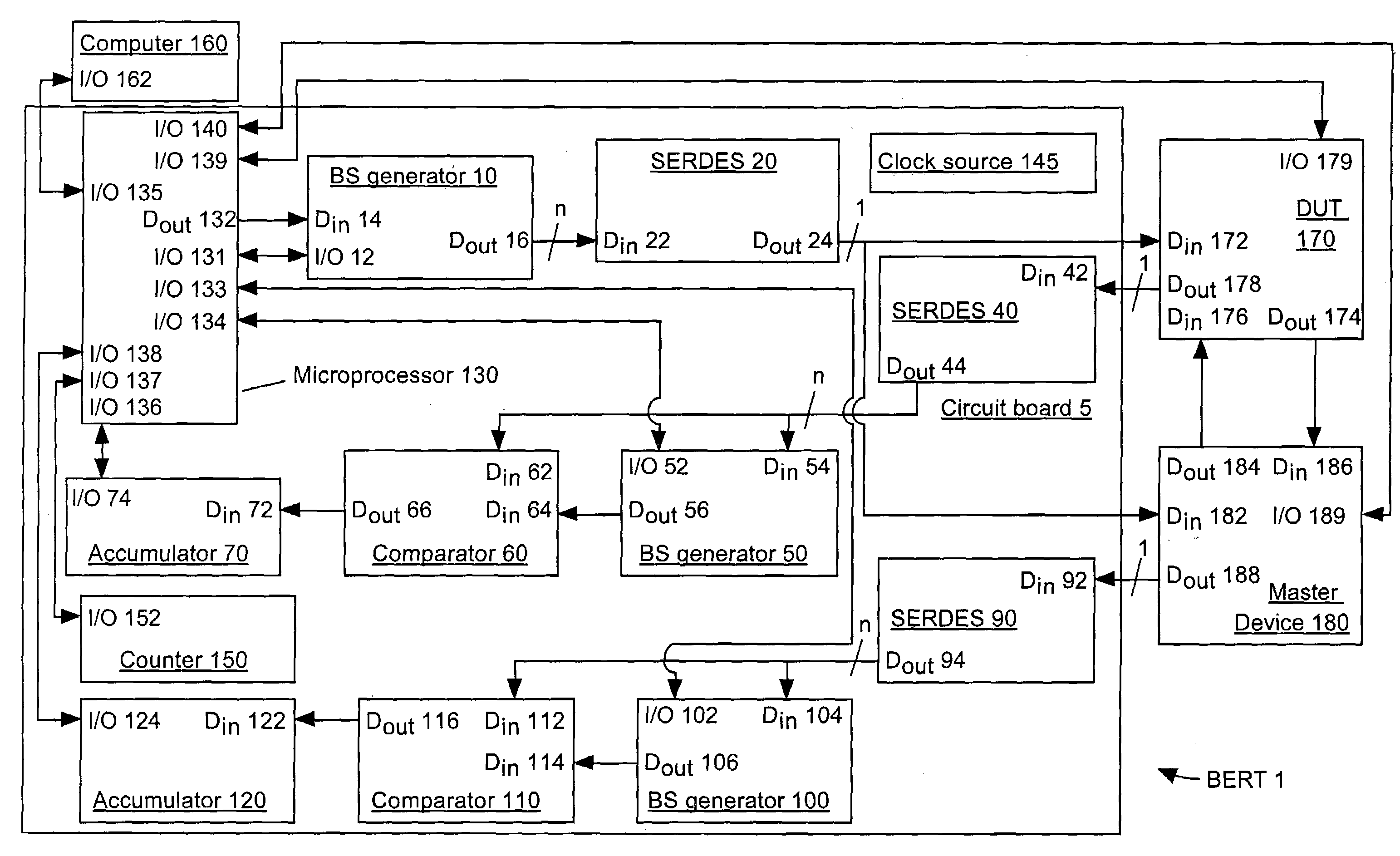
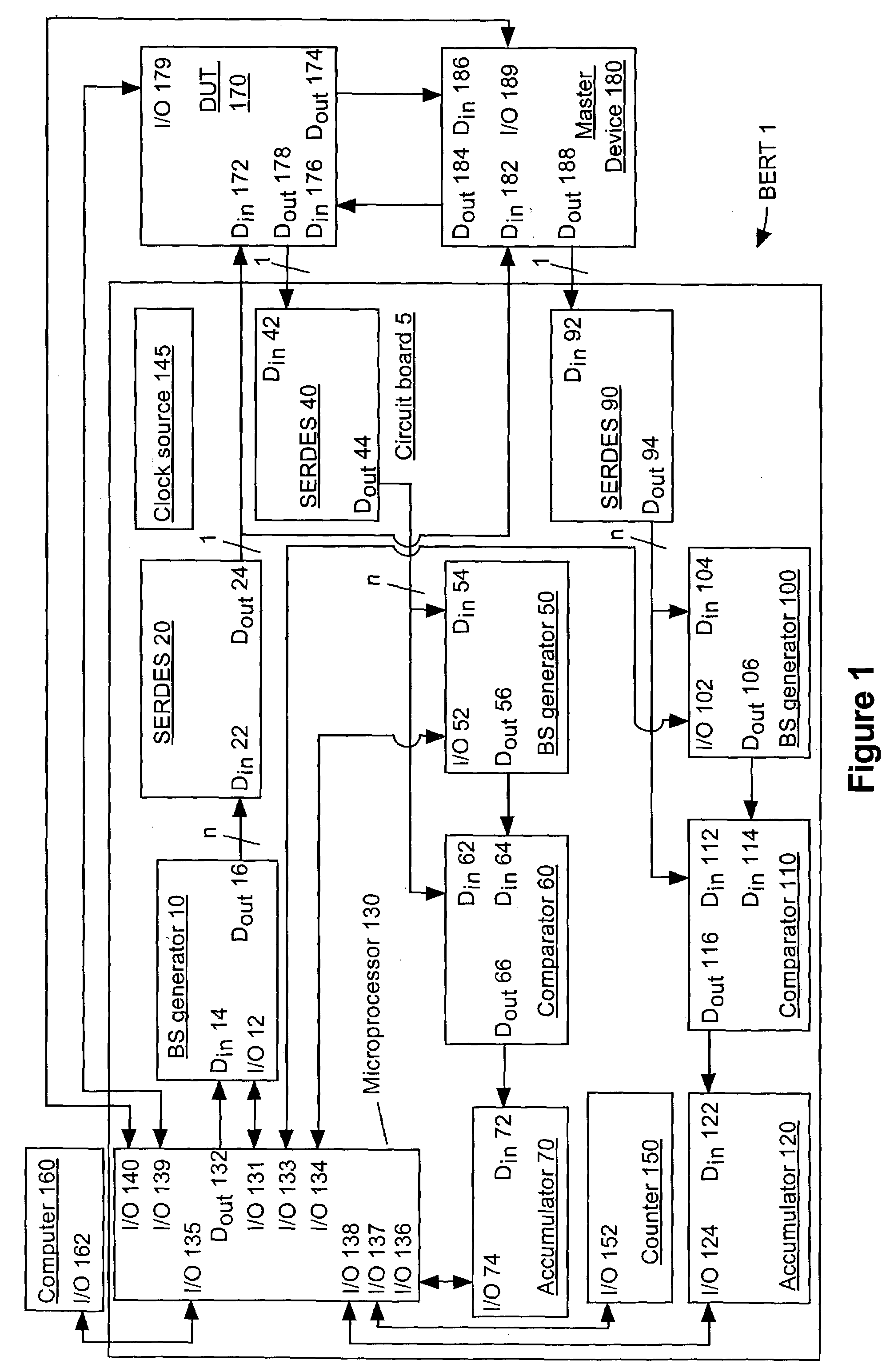
[0017]Referring to FIG. 1, there is shown a BERT 1 consistent with an embodiment of the present invention. As illustrated in FIG. 1, the BERT 1 includes a circuit board 5, a first bit sequence (“BS”) generator 10, a first serializer / deserializer (“SERDES”) 20, a second SERDES 40, a second BS generator 50, a first comparator 60, a first accumulator 70, a third SERDES 90, a third BS generator 100, a second comparator 110, a second accumulator 120, a microprocessor 130, a clock source 145, a timer 150, and a computer 160. Connected to the BERT 1, as illustrated in FIG. 1, are a device under test (“DUT”) 170 and a master device 180.

[0018]The circuit board 5 is typically an insulated board that houses interconnected circuitry. The circuit board 5 typically provides power and ground connections (not illustrated) for various components mounted thereon.

[0019]The BS generators illustrated in FIG. 1 (i.e., the first BS generator 10, the second BS generator 50, and the third BS generator 100) ...


PUM


Abstract

The present invention relates generally to an improvement in the ability of test systems to test bit processing capacities of electronic devices, and in particular an improvement in their ability to test the operation of an electronic device's transmitter and receiver circuitry. Data generated by a BERT is transmitted in an electrical form to a DUT and a master device. The DUT transmits data received in an electrical form to the master device in an optical form and the master device transmits data received in an electrical form to the DUT in an optical form. The master device and the DUT then transmit data received in an optical form back to the BERT in an electrical form. The data received from the DUT and the master device, respectively, is separately tested for bit errors. Do so enables to calculation of bit error rates for two distinguishable data paths through the DUT.

Description

[0001]The present application claims priority, under 35 U.S.C. 119(e), to a U.S. Provisional Patent Application No. 60 / 416,649, filed on Oct. 7, 2002, entitled “A SYSTEM AND METHOD OF DETECTING A BIT PROCESSING ERROR,” and incorporated herein by reference.RELATED APPLICATION[0002]The present application is related to, and incorporates by reference, a U.S. patent application Ser. No. 10 / 285,082 entitled “A SYSTEM AND METHOD OF PROCESSING A DATA SIGNAL”.BRIEF DESCRIPTION OF THE INVENTION[0003]The present invention relates generally to an improvement in the ability of test systems to test bit processing capacities of electronic devices, and in particular an improvement in their ability to test the operation of an electronic device's transmitter and receiver circuitry.BACKGROUND OF THE INVENTION[0004]A bit error rate (“BER”) is a ratio of bits received, processed, and / or transmitted with errors to a total number of bits received, processed, and / or transmitted over a given period of time...

Claims


Application Information

Patent Timeline
IPC IPC(8): G06F11/00H04B17/00H04L1/20H04L1/24
CPCH04L1/243H04B17/20H04B17/15H04L1/203
Inventor FISHMAN, ALEXHARITOS, KONSTANTINOS G.SUNG, PAULBANNIKOV, DMITRIDOROFEEV, SERGUEI
Owner II VI DELAWARE INC
Learn More