System and method for reduced power open-loop synthesis of output clock signals having a selected phase relative to an input clock signal

a clock signal and open-loop technology, applied in the field of low-power system and method, can solve the problems of inability to use a fixed timing circuit, the critical timing of the write data strobe signal, and the disadvantages of closed loop circuits, so as to achieve the effect of greatly reducing the power consumed by the measurement delay lin

Inactive Publication Date: 2006-07-18
MICRON TECH INC
View PDF48 Cites 15 Cited by
  • Summary
  • Abstract
  • Description
  • Claims
  • Application Information

AI Technical Summary

Benefits of technology

[0012]A system and method for generating an output clock signal having a selected phase shift relative to an input clock signal is generated in an open-loop manner using a measurement delay line having a plurality of delay elements and one or more signal generating delay lines having a respective sub-multiple of delay elements. An input clock signal propagates through the measurement delay line, and the delay element to which a transition of the input clock signal has propagated at the next transition of the input clock signal sets a corresponding latch. The set latch determines the number of delay element in each signal generating delay line through which a signal propagates to generate a respective output signal. The latch may remain set for a large number of cycles of the input clock signal so that it is not necessary for the input clock signal to propagate through the measurement delay line each cycle. As a result, the power consumed by the measurement delay line can be greatly decreased.

Problems solved by technology

However, as the speed of memory devices has continued to increase, the “data eye” has become smaller and smaller, thus making the timing of the write data strobe signal even more critical.
Unfortunately, the phase of the system clock signal is normally substantially the same as the phase of the write data signals.
Therefore, it is generally not practical to use a fixed timing circuit to generate a write data strobe signal from the system clock signal.
However, closed loop circuits are not without their disadvantages and limitations.
Specifically, closed loop circuits typically require a substantial amount of circuitry, which occupies space on a semiconductor die that could otherwise be used for increased memory capacity.
Furthermore, it typically requires a substantial period of time for the closed loop circuit to establish “lock” during which time the memory device cannot latch write data signals.
However, generating the necessary quadrature clock signal has the same type of difficulties that are incurred in generating a quadrature write data strobe signal.
Although this open loop clock generating system avoids many of the disadvantages of closed-loop clock generating systems, it has the disadvantage of consuming a considerable amount of power.
The high power consumption is, in part, the result of the power consumed by each cycle of the input clock signal propagating through the measurement delay line.
The power consumed by the measurement delay line is particularly high because the measurement delay line contains a large number of delay elements, each of which consumes power each time it switches.

Method used


Image

  • System and method for reduced power open-loop synthesis of output clock signals having a selected phase relative to an input clock signal
  • System and method for reduced power open-loop synthesis of output clock signals having a selected phase relative to an input clock signal
  • System and method for reduced power open-loop synthesis of output clock signals having a selected phase relative to an input clock signal

Examples


Embodiment Construction

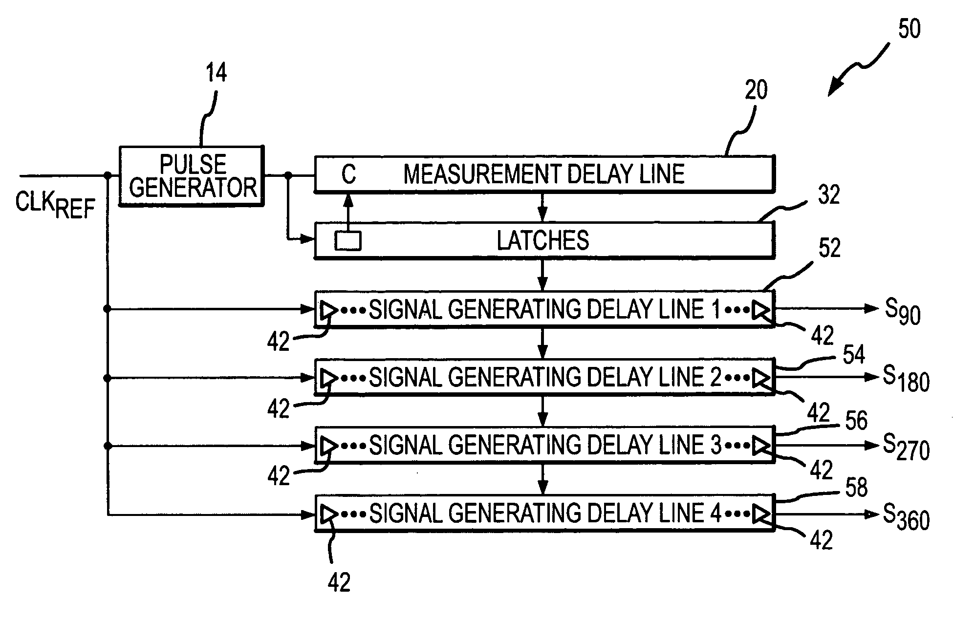
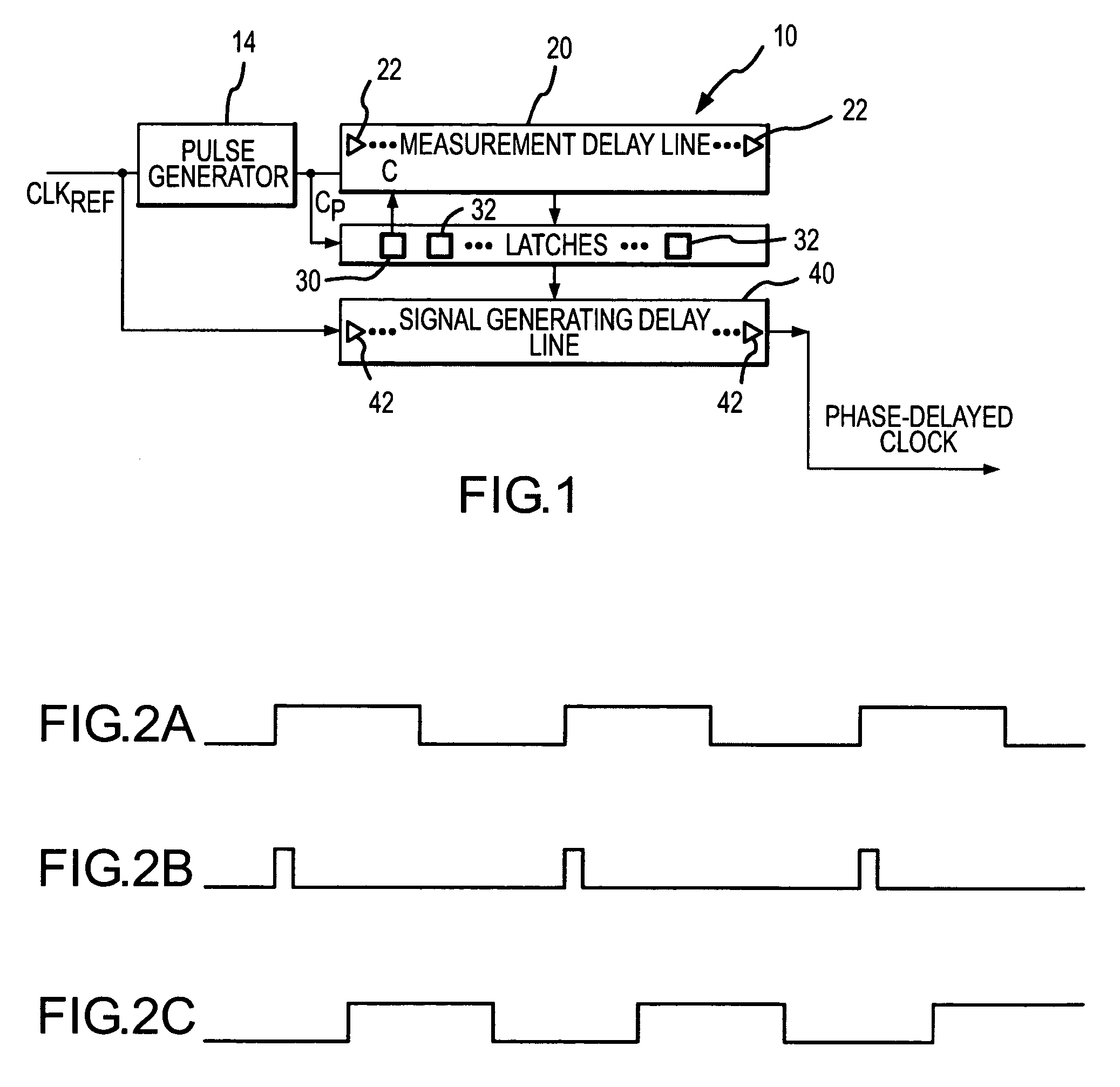
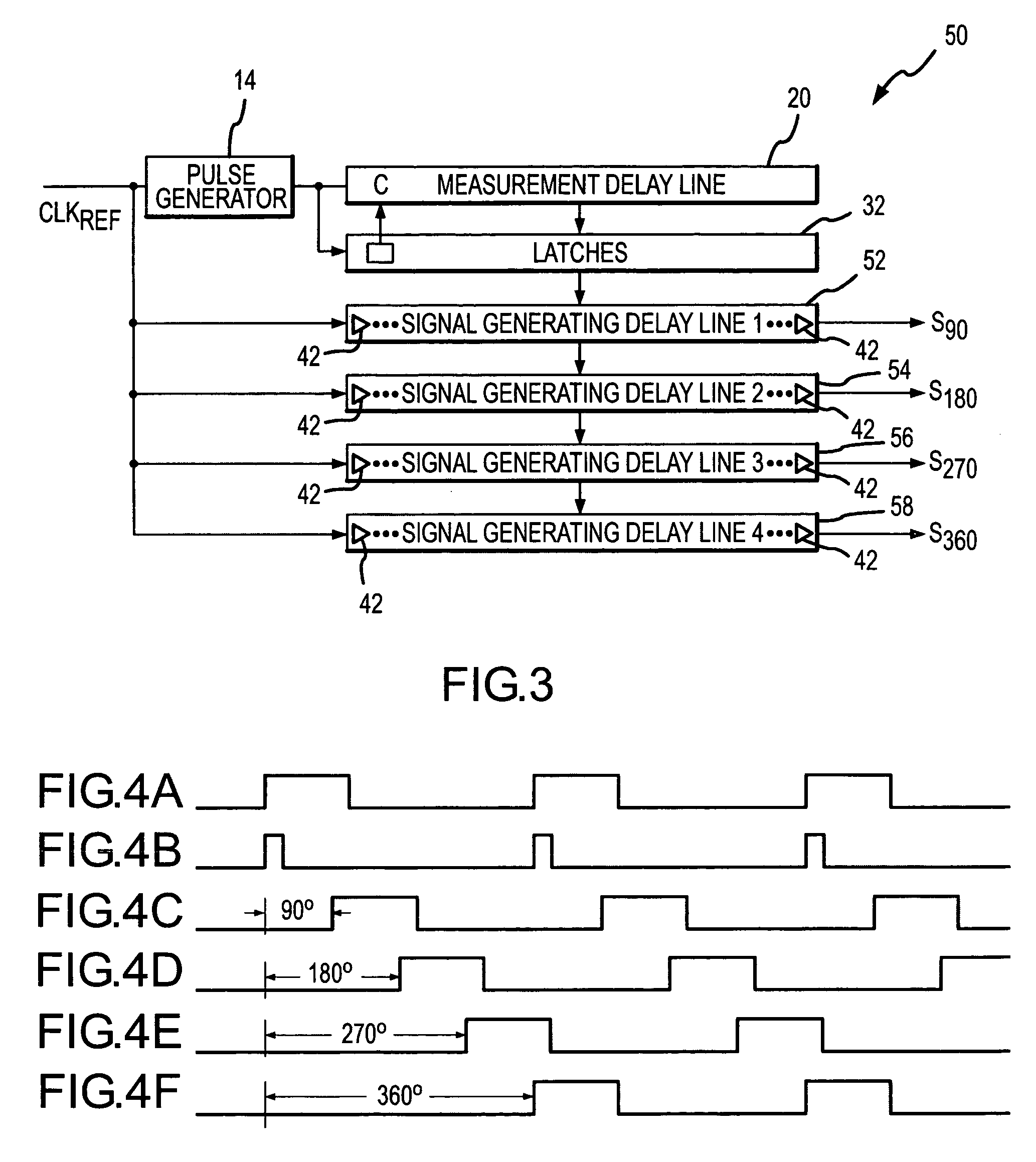
[0024]One embodiment of a signal generating circuit 10 for generating a quadrature clock signal is shown in FIG. 1. The circuit 10 receives a reference clock signal CLKREF, which is applied to one input of a pulse generator 14. The pulse generator 14 outputs a short pulse CP responsive to a predetermined transition of the CLKREF signal, such as each rising edge of the CLKREF signal. The CP pulse is applied to the input of a measurement delay line 20, which includes a large number of delay elements 22. The delay line 20 may be similar to delay lines disclosed in previously mentioned application Ser. No. 10 / 854,849, filed May 25, 2004, which is hereby incorporated by reference. The CP pulse is also preferably applied to a counter 30 associated with a set of latches 32.

[0025]The CP pulse propagates through the delay elements 22 in the measurement delay line 20 until the next transition of the CP pulse occurs. The delay element 22 to which the CP pulse has propagated at that time then s...


PUM


Abstract

A signal generating circuit includes a pulse generator generating a pulse responsive to a periodic clock reference signal. The pulse propagates through a plurality of series-connected delay elements in a measurement delay line. The measurement delay line is coupled to a series of latches that correspond to respective groups of delay elements in the measurement delay line. The delay element to which the pulse has propagated when the next pulse is received causes a corresponding latch to be set. The clock reference signal propagates through a signal generating delay line, which contains a sub-multiple of the number of delay elements in the measurement delay line, starting at a location corresponding to the set latch. The latch may remain set for a large number of periods of the clock reference signal so that it is not necessary for the clock reference signal to propagate through the measurement delay line each cycle.

Description

TECHNICAL FIELD[0001]This invention relates to clock generating systems and methods, and, more particularly, to a low power system and method for generating a clock signal that has a selected phase relative to another signal despite variations in the frequency of the other signal without using phase-lock loops, delay-lock loops and other closed-loop techniques.BACKGROUND OF THE INVENTION[0002]Periodic digital signals are commonly used in a variety of electronic devices. Probably the most common type of periodic digital signals are clock signals that are typically used to establish the timing of a digital signal or the timing at which an operation is performed on a digital signal. For example, data signals are typically coupled to and from memory devices, such as synchronous dynamic random access memory (“SDRAM”) devices, in synchronism with a clock or data strobe signal. More specifically, read data signals are typically coupled from a memory device in synchronism with a read data s...

Claims


Application Information

Patent Timeline
Patent Type & Authority Patents(United States)
IPC IPC(8): H03H11/26
CPCG11C7/106G11C7/1066G11C7/1087G11C7/1093G11C7/22G11C7/222G11C11/4076H03K5/00006H03K5/135G11C7/1027H03K2005/00286G11C7/1078G11C11/406G11C11/408G11C11/4093G11C7/1051
Inventor GOMM, TYLERZIMLICH, DAVID
Owner MICRON TECH INC
Why Eureka
Try Eureka