
Flip-chip type quad flat package and leadframe

a technology of flip-chip and leadframe, which is applied in the direction of semiconductor devices, semiconductor/solid-state device details, electrical apparatus, etc., can solve the problems of complicated conventional process of forming a solder mask on the lead, difficult control of the height of the collapsed bump b>140/b>,

Active Publication Date: 2006-06-27
ADVANCED SEMICON ENG INC
View PDF2 Cites 11 Cited by
  • Summary
  • Abstract
  • Description
  • Claims
  • Application Information

AI Technical Summary

Benefits of technology

The design effectively prevents bump collapse and stabilizes bump height, simplifies the production process, and reduces costs by eliminating the need for a solder mask, while maintaining electrical connectivity between bonding pads and leads.

Problems solved by technology

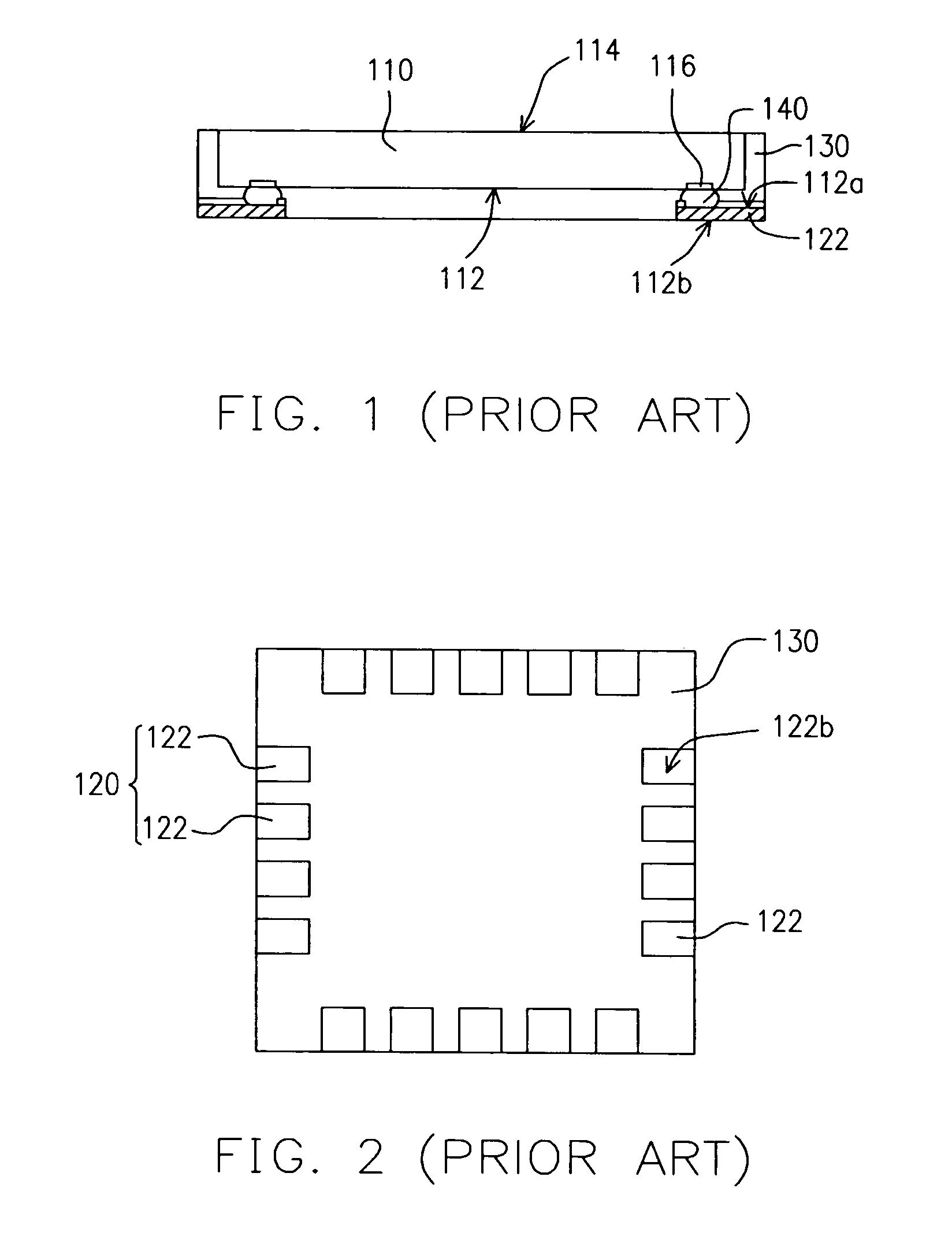
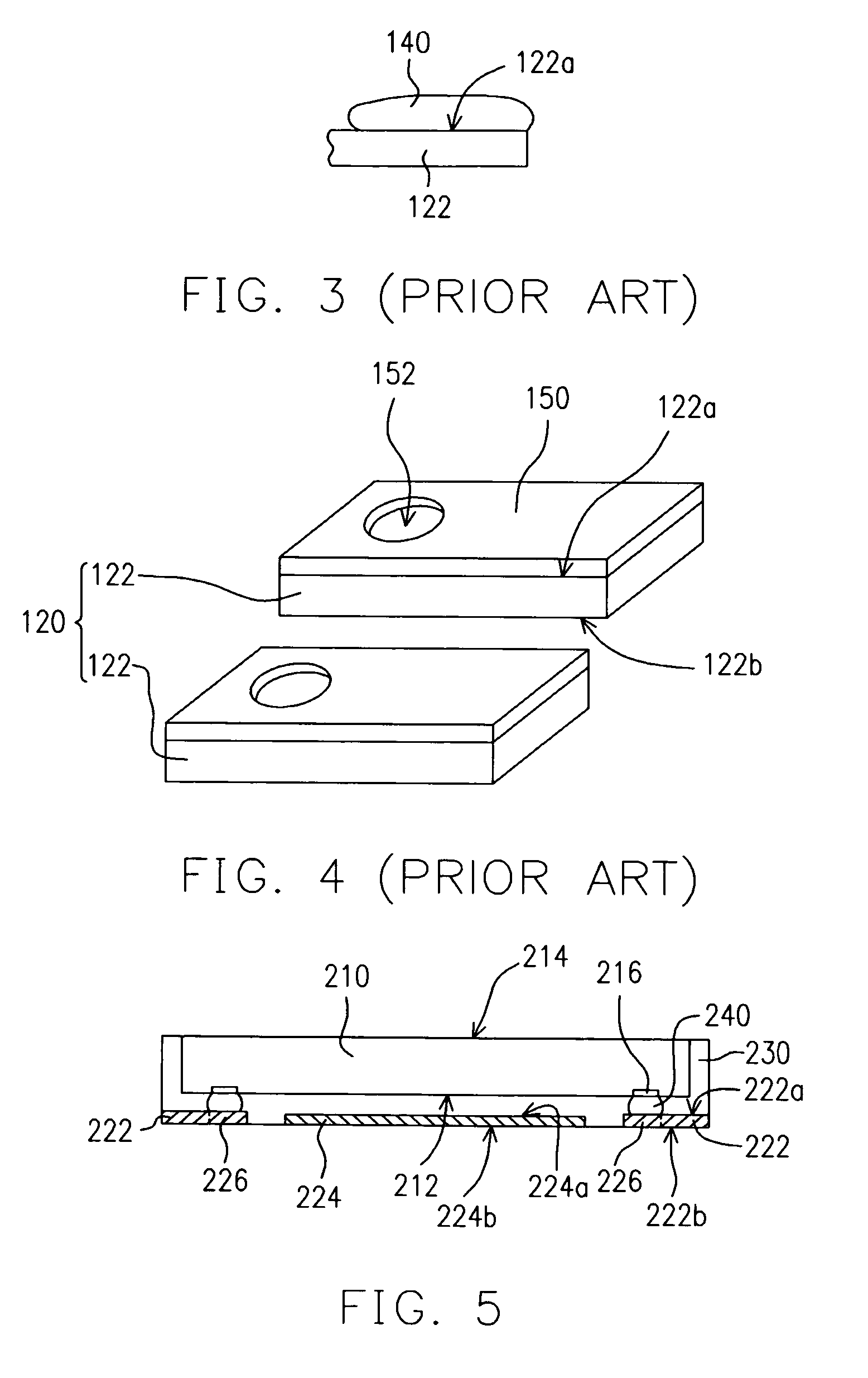
Ultimately, the height of the collapsed bump 140 is hard to control.
However, the conventional process of forming a solder mask on the leads is complicated (need to pattern the solder mask to form openings) and expensive.

Method used


Image

  • Flip-chip type quad flat package and leadframe
  • Flip-chip type quad flat package and leadframe
  • Flip-chip type quad flat package and leadframe

Examples


Embodiment Construction

[0026]Reference will now be made in detail to the present embodiments of the invention, examples of which are illustrated in the accompanying drawings. Wherever possible, the same reference numbers are used in the drawings and the description to refer to the same or like parts.

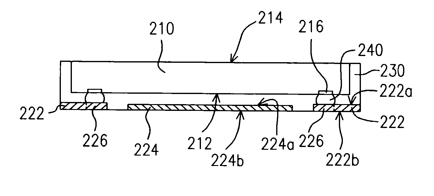
[0027]FIG. 5 is a side view of a flip-chip type quad flat package according one embodiment of the present invention. FIG. 6 is a bottom view of the flip-chip type quad flat package shown in FIG. 5. As shown in FIGS. 5 and 6, the quad flat non-leaded chip package 200 of the present invention mainly comprises a chip 210, a leadframe 220 and an encapsulant 230. The chip 210 has an active surface 212 and a corresponding back surface 214. The active surface 212 is a surface where the active devices are formed. The active surface 212 of the chip 210 further comprises a plurality of exposed bonding pads 216.

[0028]The leadframe 220 comprises a plurality of leads 222. Each lead 222 has a top surface 222a and a bottom s...


PUM


Abstract

A flip-chip type quad flat package and a leadframe. The leadframe comprises a bump-connecting area and a non-connecting area. The maximum width of the bump-connecting area is larger than the width of the non-connecting area. A bump is limited to the bump-connecting area after performing a reflow process so that the bumps are prevented from collapsing, the manufacturing cost is reduced and the process is simplified.

Description

CROSS-REFERENCE TO RELATED APPLICATION[0001]This application claims the priority benefit of Taiwan application serial no. 92130406, filed on Oct. 31, 2003.BACKGROUND OF THE INVENTION[0002]1. Field of the Invention[0003]The present invention relates to a flip-chip type quad flat package (FC-QFP) and a leadframe. More particularly, the present invention relates to a flip-chip type quad flat package and a leadframe that can prevent abnormal collapse of bumps, lower the production cost and simplify the production process.[0004]2. Description of the Related Art[0005]The techniques for fabricating semiconductor devices are progressing at a rapid pace. With great advances in production techniques, many types of customized, multi-functional and yet compact and handy electronic products have been developed. In the semiconductor fabrication industry, leadframe is still one of the most commonly used carriers. According to the configuration of the leads in a leadframe, a quad flat package (QFP)...

Claims


Application Information

Patent Timeline
Patent Type & Authority Patents(United States)
IPC IPC(8): H01L23/495H01L23/48H01L23/31
CPCH01L23/4951H01L23/49541H01L23/4952H01L23/3107H01L2224/16H01L23/49568H01L2224/05571H01L2224/05573
Inventor WANG, HSUEH-TEWANG, MENG-JENCHIU, CHI-HAOLIU, CHIEN
Owner ADVANCED SEMICON ENG INC
Learn More