Display device

a technology of a display device and a display plate, which is applied in the direction of identification means, semiconductor/solid-state device details, instruments, etc., can solve the problems of too low drive voltage at the area of pixels, too high resistance, and parts of the conductor pattern on the first substrate become so long

Inactive Publication Date: 2006-06-20
VIDA SENSE INNOVATION LTD
View PDF18 Cites 4 Cited by
  • Summary
  • Abstract
  • Description
  • Claims
  • Application Information

AI Technical Summary

Benefits of technology

[0004]It is, inter alia, an object of the invention to provide a display device, in which, in a reliable manner, the surface of the first substrate is provided with low-ohmic conductors which are connected to the exterior while simultaneously obtaining a maximum freedom of design.
[0009]Another embodiment of a display device according to the invention is characterized in that electrically conducting patterns on both sides of the foil form a cross-connection. The use of such cross-connections further increases the number of possibilities of designing the circuit to be realized on the foil.

Problems solved by technology

Parts of the conductor pattern on the first substrate then become so long that, due to their length, they have a too high resistance.
The voltage loss caused thereby leads to too low drive voltages at the area of the pixels, which is at the expense of the correct adjustment of the grey scale or may even lead to non-excitation of the pixel.

Method used


Image

  • Display device
  • Display device
  • Display device

Examples


Embodiment Construction

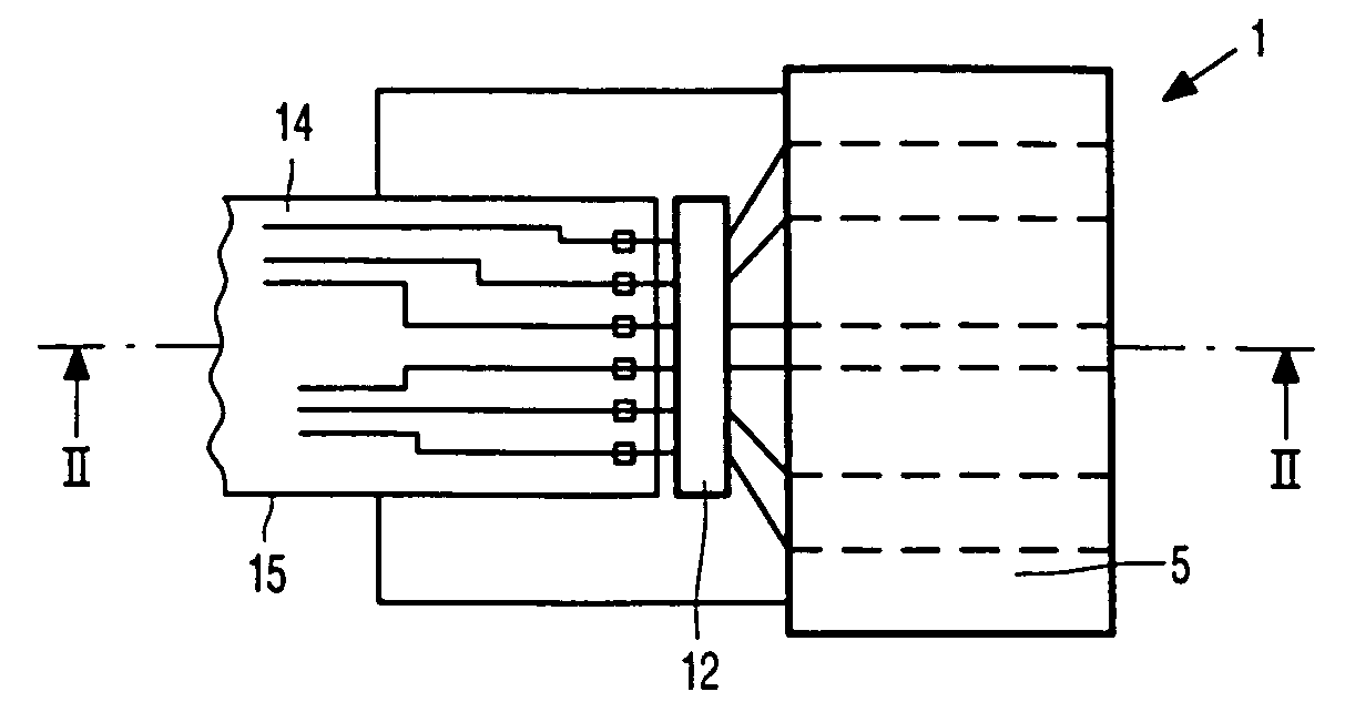
[0021]FIG. 1 is a diagrammatic plan view and FIG. 2 is a cross-section of a part of a display device, in this example a liquid crystal display device comprising a liquid crystal cell 1 with a twisted nematic liquid crystal material 2 which is present between first and second transparent substrates 3, 4 of, for example, glass or synthetic material, provided with electrodes 5, 6 in this embodiment. The device further comprises polarizers (not shown) whose direction of polarization is, for example, mutually crossed perpendicularly. The device also comprises orientation layers (not shown) which orient the liquid crystal material on the inner walls of the substrates, in this embodiment in such a way that the cell has a twist angle of 90 degrees. In this embodiment, the liquid crystal material has a positive optical anisotropy and a positive dielectric anisotropy. When the electrodes 5, 6 are energized with an electric voltage, the molecules, and hence the directors, direct themselves to ...


PUM

PropertyMeasurementUnit
twist angleaaaaaaaaaa
electrically conductingaaaaaaaaaa
areaaaaaaaaaaa

Abstract

A flexible foil having double-sided conductor patterns of a satisfactorily conducting material (gold, silver, nickel) is used in the interconnection of conductor patterns of a display device (LCD, OLED), which enhances the freedom of design.

Description

BACKGROUND OF THE INVENTION[0001]The invention relates to a display device comprising a first substrate which is provided with a conductor pattern for connecting pixels in an electrically conducting manner. A conductor pattern may be understood to mean both a pattern of exclusively column and row conductors and a more extensive pattern in which drive ICs are incorporated.[0002]Such display devices, notably liquid crystal display devices, are very generally used in, for example, measuring equipment but also in, for example, portable telephones. Moreover, electroluminescent display devices based on (organic) LEDs find an increasingly wider application.[0003]With the on-going miniaturization of electronics, it is possible, on the one hand, to realize more standard drive electronics on the substrate. On the other hand, the need for offering customer-oriented solutions, realizing, for example extra functions, increases simultaneously. Parts of the conductor pattern on the first substrate...

Claims


Application Information

Patent Timeline
Patent Type & Authority Patents(United States)
IPC IPC(8): G09G3/36G02F1/1345G02F1/13G09F9/00G09F9/30H01L23/498H05K3/36
CPCH01L23/4985G02F1/13452H01L2224/16H01L2224/16225H01L2924/12044H05K3/361H01L2924/01079H01L2924/00014H01L2224/0401
Inventor TRIEPELS, JOZEPH W.KUSTERS, ROEL H. L.VERWEG, FRANSISCUS G. C.HANDELS, HENRI S. A.BACHUS, MARCEL S. B.SCHEUERMANN, JOHANNES W. J. M.
Owner VIDA SENSE INNOVATION LTD
Why Eureka
Try Eureka