
Inspection method and inspection apparatus

a technology of inspection apparatus and inspection method, which is applied in the direction of semiconductor/solid-state device testing/measurement, instruments, material electrochemical variables, etc., can solve the problems of contaminated devices with scraped dust, inability to ensure the electrical contact between the probe and the inspection electrode, and inability to apply force, etc., to reduce the necessity of application, prolong the life of the probe, and suppress the damage done

Inactive Publication Date: 2006-06-13
TOKYO ELECTRON LTD +2
View PDF13 Cites 5 Cited by
  • Summary
  • Abstract
  • Description
  • Claims
  • Application Information

AI Technical Summary

Benefits of technology

[0012]In the method in which the tip of the probe is stuck into the inspection electrode, the damage done to the inspection electrode is small. However, the inspection electrode is scratched as in the method described above. Also required is the durability for maintaining the shape of the tip portion of the probe. Since the degree of integration of the devices has been markedly enhanced in recent years, the miniaturization of the device and the thinning of the film have been drastically progressed. Under the circumstances, the thickness of the inspection electrode has been decreased such that, if the probe is stuck until the probe is brought into electrical contact with the inspection electrode, the underlying layer of the inspection electrode also tends to be damaged.
[0015]An object of an aspect of the present invention is to provide an inspection method and an inspection apparatus, which permit markedly decreasing the needle pressure applied by the probe to the measuring electrode.
[0031]Another object of an aspect of the present invention is to provide an inspection method and an inspection apparatus, which permit suppressing the damage done to the inspection electrode and which also prolong the life of the probe when used repeatedly.
[0032]Still another object of an aspect of the present invention is to provide an inspection method and an inspection apparatus which reduce the necessity of applying a cleaning treatment to the probe so as to improve the inspecting efficiency.

Problems solved by technology

In the method of scraping off the insulating film, it is possible for the scraped dust of the insulating film to attach to the probe N, which impairs conduction.
Therefore, it is not guaranteed that electrical contact between the probe and the inspection electrode can be ensured by the method described above.
It has also been found that the device is contaminated with the scraped dust scattered from the insulating film O, as shown in FIG. 22B.
Such being the situation, it is necessary to periodically remove the scraped dust of the insulating film from the probe N, leading to a reduction in the inspection efficiency.
In the method in which the tip of the probe is stuck into the inspection electrode, the damage done to the inspection electrode is small.
However, the inspection electrode is scratched as in the method described above.
Under the circumstances, the thickness of the inspection electrode has been decreased such that, if the probe is stuck until the probe is brought into electrical contact with the inspection electrode, the underlying layer of the inspection electrode also tends to be damaged.
The probe card manufactured by utilizing the micro machine processing technology has a fine probe structure, with the result that it is difficult to apply a high needle pressure to the probe.

Method used


Image

  • Inspection method and inspection apparatus
  • Inspection method and inspection apparatus
  • Inspection method and inspection apparatus

Examples


Embodiment Construction

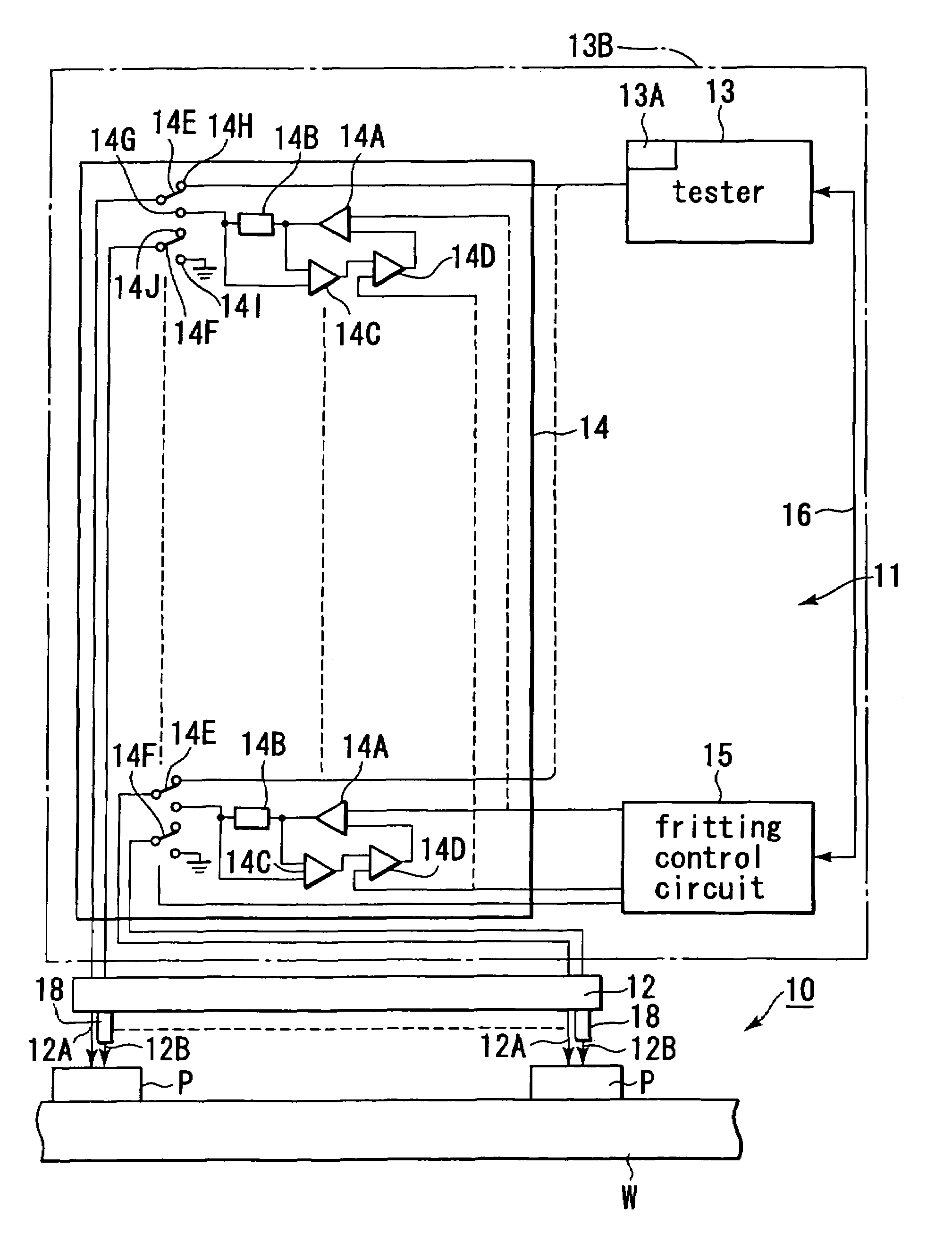
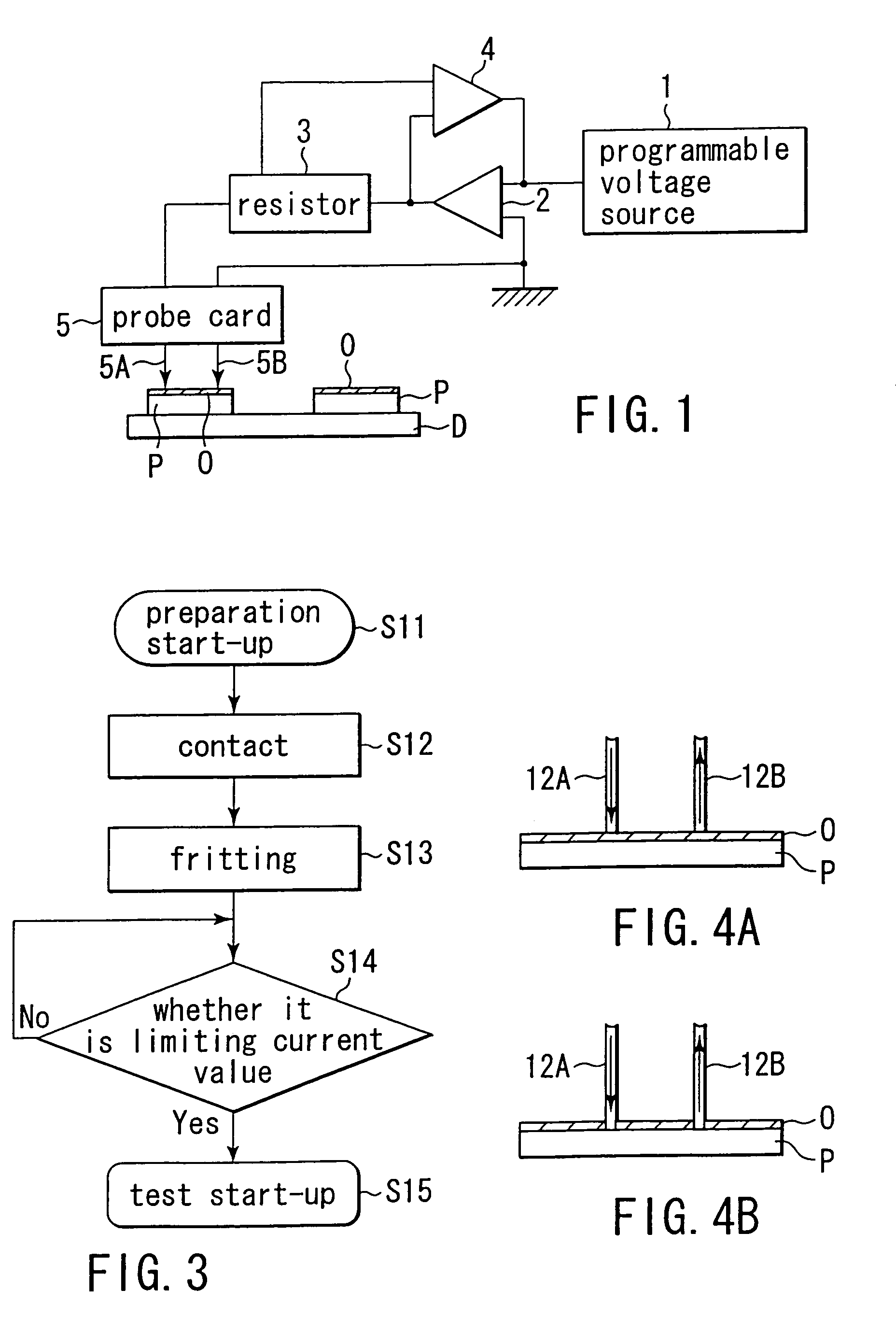
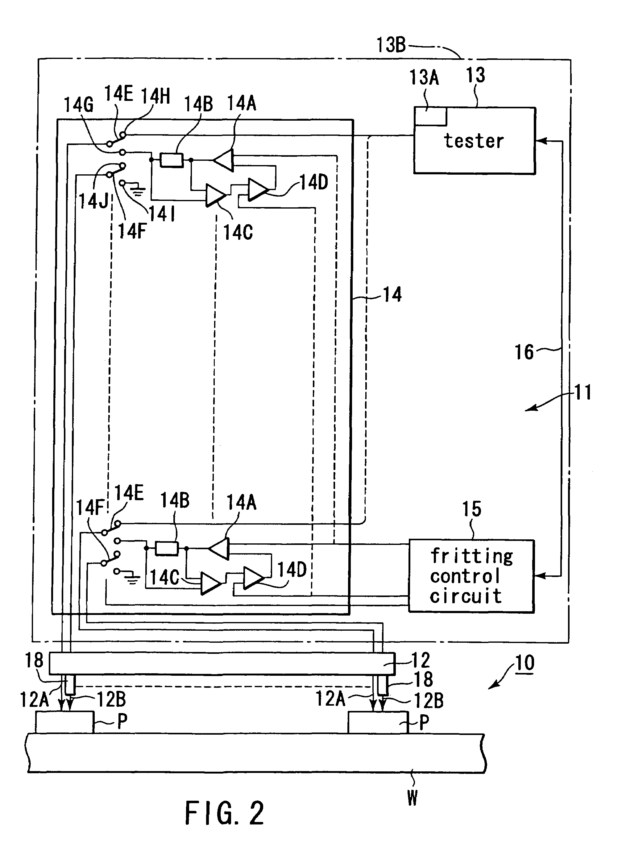
[0086]FIGS. 1 to 5 collectively show a first embodiment of the present invention. In the inspection method of the embodiment, a part of the insulating film such as an oxide film formed on the surface of the inspection electrode of the device is broken by utilizing a fritting phenomenon. In the embodiment, the probe is brought into electrical contact with the inspection electrode in the portion where the insulating film is broken. It is possible to lower the needle pressure between the probe and the inspection electrode to a level lower than the present level of the needle pressure, i.e., the needle pressure can be lowered to, for example, 0.1 g or less, by utilizing the fritting phenomenon. As a result, the inspection electrode is not scratched so as to prolong the life of the probe. The fritting phenomenon denotes the phenomenon that, if a voltage is applied to the insulating film such as an oxide film formed on the surface of a metal, i.e., the inspection electrode in the embodime...


PUM

PropertyMeasurementUnit
currentaaaaaaaaaa
displacementaaaaaaaaaa
currentaaaaaaaaaa

Abstract

Disclosed is an inspection method for inspecting the electrical characteristics of a device by bringing an inspecting probe into electrical contact with an inspection electrode. An insulating film formed on the surface of the inspection electrode is broken by utilizing a fritting phenomenon so as to bring the inspection electrode into electrical contact with the inspection electrode.

Description

[0001]This application is a Division of application Ser. No. 09 / 931,888 filed on Aug. 20, 2001 now U.S. Pat. No. 6,777,967.CROSS-REFERENCE TO RELATED APPLICATIONS[0002]This application is based upon and claims the benefit of priority from the prior Japanese Patent Applications No. 2000-249702, filed Aug. 21, 2000; and No. 2001-093303, filed Mar. 28, 2001, the entire contents of both of which are incorporated herein by reference.BACKGROUND OF THE INVENTION[0003]1. Field of the Invention[0004]The present invention relates to an inspection method and an inspection apparatus, particularly, to an inspection method and an inspection apparatus which permit suppressing the needle pressure applied by a probe to the inspection electrode of a target object to be inspected.[0005]2. Description of the Related Art[0006]In the manufacturing process of semiconductor devices, these devices are formed on a semiconductor wafer. Then, inspected are the electrical characteristics of the target object(s)...

Claims


Application Information

Patent Timeline
Patent Type & Authority Patents(United States)
IPC IPC(8): G01R31/02G01N27/30G01R31/26G01R1/06G01R1/067G01R31/28H01L21/66
CPCG01R1/067G01R31/2891G01R31/2886G01R1/06794G01R3/00G01N27/30
Inventor IINO, SHINJITAKEKOSHI, KIYOSHISUGAITOHKATAOKA, KENICHI
Owner TOKYO ELECTRON LTD
Learn More