
Manufacture method of pixel structure

Active Publication Date: 2006-05-23
CHUNGHWA PICTURE TUBES LTD
View PDF13 Cites 8 Cited by
  • Summary
  • Abstract
  • Description
  • Claims
  • Application Information

AI Technical Summary

Benefits of technology

[0023]In the manufacture method of pixel structure of the invention, while the dry etching is performed to pattern the semiconductor layer, since the first mask layer and the second mask layer are both serving as the etching mask, the drain electrode is not bombard by the plasma. As a result, the contact impedance between the drain electrode and the pixel electrode can be reduced, so that the yield can increase, and the displaying quality of the TFT-LCD can be improved. In addition, the first mask layer and the second mask layer can be simultaneously removed in the manufacture method of pixel structure of the invention. Thus, the invention can save one step of removing the mask layer, so that the throughput is improved.
[0024]Further still, in another manufacture method of pixel structure of the invention, the second mask over the source / drain electrodes is fully covering the source / drain electrodes and the region between the source / drain electrodes. Whereby, the drain electrode is bombard by the plasma while patterning the semiconductor layer by dry etching. As a result, the contact impedance between the drain electrode and the pixel electrode can be reduced, so that the yield can increase, and the displaying quality of the TFT-LCD can be improved.

Problems solved by technology

This may also cause the poor performance for the TFT displaying device.

Method used


Image

  • Manufacture method of pixel structure
  • Manufacture method of pixel structure
  • Manufacture method of pixel structure

Examples


first embodiment

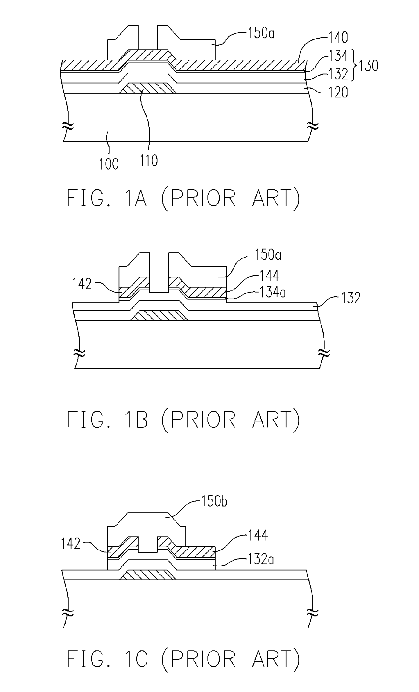
[0029]FIGS. 2A–2G are cross-sectional views, schematically illustrating the manufacture process flow for a pixel structure, according to a first embodiment of the invention. In FIG. 2A, a gate electrode 110 is formed over a substrate 100. Wherein, the material of the gate electrode 110 includes, for example, Cr, Al, Mo or other suitable metallic material.

[0030]In FIG. 2B, a gate insulating layer 120 is formed over the substrate 100, and covers the gate electrode 110. After then, a semiconductor layer 130 is formed over the gate insulating layer 120. Wherein, the method for forming the semiconductor 130 includes, for example, forming a channel material layer 132 over the gate insulating layer 132. In addition, the gate insulating layer 120 includes, for example, silicon nitride. The channel material layer 132 includes, for example, amorphous silicon. The ohm contact material layer 134 includes, for example, n-type amorphous silicon. It should be noted that the ohm contact material la...

second embodiment

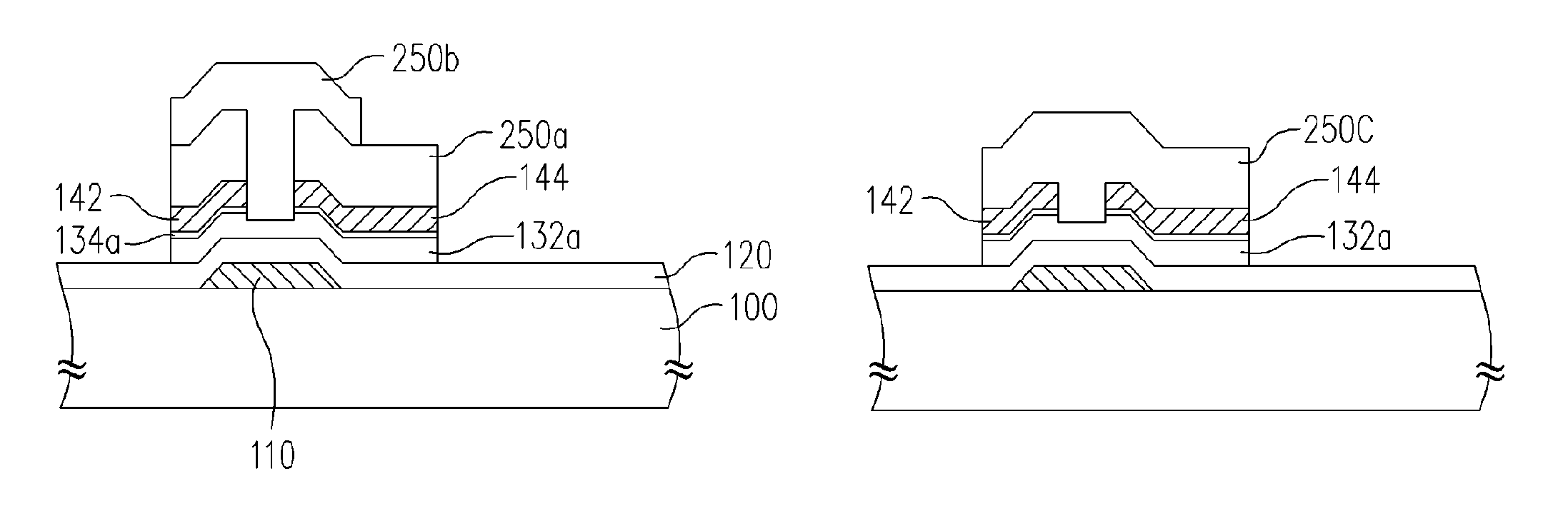
[0037]FIGS. 3A–3E are cross-sectional views, schematically illustrating the manufacture process flow for a pixel structure, according to a second embodiment of the invention. In FIGS. 3A–3E, the manufacture method of pixel structure in the second embodiment mainly includes the following steps. In FIG. 3A, using the steps in FIGS. 2A–2C to form a gate electrode 110 over the substrate 100. A gate insulating layer 120 is formed over the substrate 100. And then, a semiconductor layer 130 is formed over the gate insulating layer 120. Wherein, the method for forming the semiconductor layer 130 includes, for example, forming a channel material layer 132 over the gate insulating layer 120, and forming an ohm contact material layer 134 over the channel material layer 132. A metal layer 140 is formed over the semiconductor layer 130, and a mask layer 250a is formed over the metal layer 140.

[0038]In FIG. 3B, the mask layer 250a is used as the etching mask, so as to pattern the metal layer 140 ...


PUM


Abstract

A manufacture method of a pixel structure is provided. A gate is formed over a substrate, and a gate insulator layer is formed over the substrate covering the gate. A semiconductor layer is formed over the gate insulator layer and a metal layer is formed over the semiconductor layer. A first mask layer is formed on the metal layer, and the metal layer is patterned to form a source / drain by using the first mask layer as etching mask. Afterward, a second mask layer is formed on the first mask layer and further covers a region between the source / drain. The semiconductor layer is patterned by using the first and second mask layers as etching mask, and then the first and second mask layers are removed. A passivation layer is formed over the substrate. A pixel electrode is formed on the passivation layer. The pixel electrode is electrically connected with the drain.

Description

BACKGROUND OF THE INVENTION[0001]1. Field of Invention[0002]The present invention relates to a manufacture method for a structure of semiconductor device. More particularly, the present invention relates to a manufacture method for a pixel structure of a thin-film transistor (TFT) liquid crystal display (LCD).[0003]2. Description of Related Art[0004]As a fact of rapid improvement in the multi-media society, it mainly is due to the benefits of great development on the semiconductor devices or the displaying device. With respect to the displaying device, the TFT-LCD with great properties of high image quality, high efficiency of space use, low power consumption and radiation has gradually become a main trend in the market.[0005]The TFT-LCD is mainly composed of a TFT-array substrate, a color-filter-array substrate, and liquid crystal layer, wherein the TFT-array includes multiple TFT's arranged in an array manner, and pixel electrodes respectively implemented with TFT, so as to form m...

Claims


Application Information

Patent Timeline
IPC IPC(8): H01L21/28
CPCH01L27/1288H01L27/124
Inventor KAO, CHIN-TZUSU, TA-JUNGLIN, FU-LIANG
Owner CHUNGHWA PICTURE TUBES LTD
Learn More