
Adhesive and electric device

Active Publication Date: 2006-05-09
SONY CORP
View PDF13 Cites 0 Cited by
  • Summary
  • Abstract
  • Description
  • Claims
  • Application Information

AI Technical Summary

Benefits of technology

[0008]The invention has been created to solve the disadvantages associated with the conventional techniques, and an object thereof is to provide an adhesive of high reliability.
[0013]As the presence of a filler is indispensable for decreasing the thermal expansion coefficient and the absorbability of the adhesive, the inventors of the invention have paid attention to a filler material, and as a result of cumulative investigations, they have found a method for improving the cohesive force of filler particles by making the particle diameter of the filler particles contained in the filler material nonuniform.
[0015]Symbol 57 in FIG. 5 and FIG. 6 denotes positions where the filler particles 50 having large diameters are in contact with each other, and symbol 58 in FIG. 6 denotes positions where the filler particle 50 having large diameters and the filler particles 55 having small diameters are in contact with each other. In the case shown in FIG. 6, the number of the positions 57 and 58 where the filler particles 50 and 55 are in contact with each other is large in comparison to the case shown in FIG. 5, and thus the frictional caused by the contact of the filler particles 50 and 55 is also increased. As a result of the fact that the filler particles are packed at a high density to increase the frictional force thus formed, the cohesive force of the filler material is increased, and therefore, the rigidity of the entire adhesive is improved.
[0022]Therefore, the frictional force caused by contact of the filler particles is increased, and the rigidity of the hardened adhesive of the invention is increased.
[0023]The filler material having a particle diameter distribution having the first and second peaks can be easily produced by mixing two kinds of filler components having average particle diameters different from each other. It is also possible that one kind of filler is partially pulverized to make the particle diameter nonuniform to form the filler material.

Problems solved by technology

When the internal stress exceeds the cohesive force for forming aggregate of the adhesive, cracks and the like are formed in the adhesive to break the aggregate of the adhesive.

Method used


Image

  • Adhesive and electric device
  • Adhesive and electric device
  • Adhesive and electric device

Examples


example 1

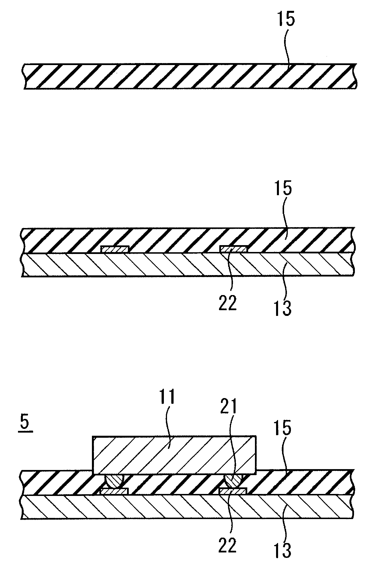
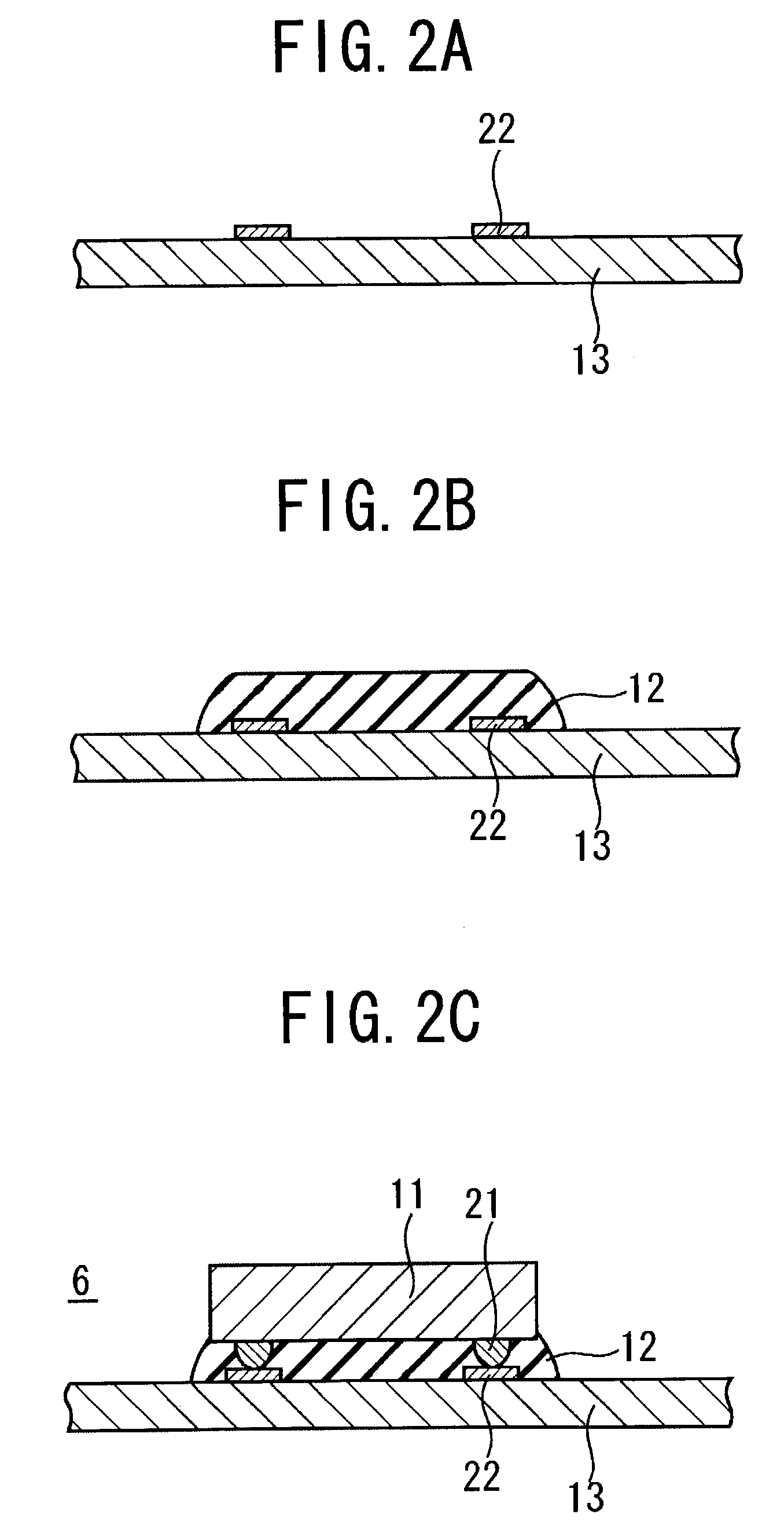
[0034]To 60 parts by weight of an epoxy resin as a thermosetting resin material, 30 parts by weight of electroconductive particles (diameter: 5 μm) formed with resin particles having a gold plating layer and a nickel plating layer (metal plating resin particles) and 60 parts by weight of a filler material formed with two kinds of filler components having average particle diameters different from each other were added, and they were sufficiently mixed to obtain an adhesive in a paste state. Silica having an average particle diameter of 1.6 μm (filler component A) and silica having an average particle diameter of 0.9 μm (filler component B) were used as a filler herein, and a mixture formed by adding 1 part by volume of the filler component B to 2 parts by volume of the filler component A was used as the filler material.

[0035]Subsequently, the adhesive is shaped into a film form to produce an adhesive film formed with the adhesive of the invention. Symbol 15 in FIG. 1A denotes the adh...


PUM

PropertyMeasurementUnit
Lengthaaaaaaaaaa
Lengthaaaaaaaaaa
Lengthaaaaaaaaaa

Abstract

The particle diameter distribution of the filler material added to the adhesive of the invention has the first peak and the second peak positioned on a side of smaller particle diameters with respect to the first peak by 0.7μ or more, and thus the rigidity of the hardened adhesive is improved. Therefore, the connection reliability of the electric device 5 having the semiconductor chip 11 and the substrate 13 by using the adhesive (adhesive film 15) is improved.

Description

TECHNICAL FIELD[0001]The present invention relates to an adhesive, and particularly relates to an adhesive for connecting a semiconductor chip to a substrate.BACKGROUND ART[0002]An adhesive formed with a thermosetting resin or a thermoplastic resin has been used to adhere a semiconductor chip to a substrate.[0003]In FIG. 7, numeral 101 denotes an electronic device containing a semiconductor chip 111 attached to a substrate 113 with an adhesive 112. A bump terminal 121 of the semiconductor chip 111 is in contact with a terminal 122 formed with a part of a wiring pattern on the substrate 113. Under the conditions, an inner circuit of the semiconductor chip 111 is electrically connected to the wiring pattern on the substrate 113 through the terminals 121 and 122. A resin constituting the adhesive 112 has been hardened, and the semiconductor chip 111 and the substrate 113 are mechanically connected to each other with the adhesive 112.[0004]However, because the thermal expansion coeffici...

Claims


Application Information

Patent Timeline
IPC IPC(8): H01B1/00H01L23/58C09J7/00C08L63/00C09J9/02C09J11/04C09J201/00H01L21/52H01L21/56
CPCC09J9/02H01L24/32H01L24/29C09J11/04H01L21/563C08L63/00H01L2924/10253H01L2924/01087H01L2924/01045H01L2924/01019H01L2924/01006H01L2224/32225H01L2924/3011H01L2924/19043H01L2924/01082H01L2924/01079H01L2924/01078H01L2924/01074H01L2924/01057H01L2924/01047H01L2924/0104H01L2224/16225H01L2224/73203H01L2224/73204H01L2224/83101H01L2224/83192H01L2224/83856H01L2924/01004H01L2924/01005H01L2924/01013H01L2924/0102H01L2924/01027H01L2924/01029H01L2924/0103H01L2924/01033H01L2924/00H01L2924/3512H01L2924/12042H01L2924/351
Inventor AKUTSU, YASUSHI
Owner SONY CORP
Learn More