
Electron beam apparatus, a pattern evaluation method and a device manufacturing method using the electron beam apparatus or pattern evaluation method

a technology of electron beam and electron beam, applied in the direction of material analysis using wave/particle radiation, instruments, nuclear engineering, etc., can solve problems such as great aberration

Inactive Publication Date: 2006-03-14
EBARA CORP
View PDF3 Cites 11 Cited by
  • Summary
  • Abstract
  • Description
  • Claims
  • Application Information

AI Technical Summary

Benefits of technology

This approach allows for low-cost manufacturing, reduced aberration, increased throughput, and efficient pattern evaluation with smaller memory storage needs, enabling high-resolution inspections of substrates with minimal line widths.

Problems solved by technology

If the electromagnetic deflector is employed as the deflector for scanning the sample, in the phase where the primary beam is deflected by that deflector to the left, for example, those returning secondary electrons are deflected to the opposite direction to the primary beam, or to the right, and resultantly the secondary electrons go away from the optical axis and enter the first lens of the secondary optical system in a position far from the optical axis, leading to a greater aberration.

Method used


Image

  • Electron beam apparatus, a pattern evaluation method and a device manufacturing method using the electron beam apparatus or pattern evaluation method
  • Electron beam apparatus, a pattern evaluation method and a device manufacturing method using the electron beam apparatus or pattern evaluation method
  • Electron beam apparatus, a pattern evaluation method and a device manufacturing method using the electron beam apparatus or pattern evaluation method

Examples


first embodiment

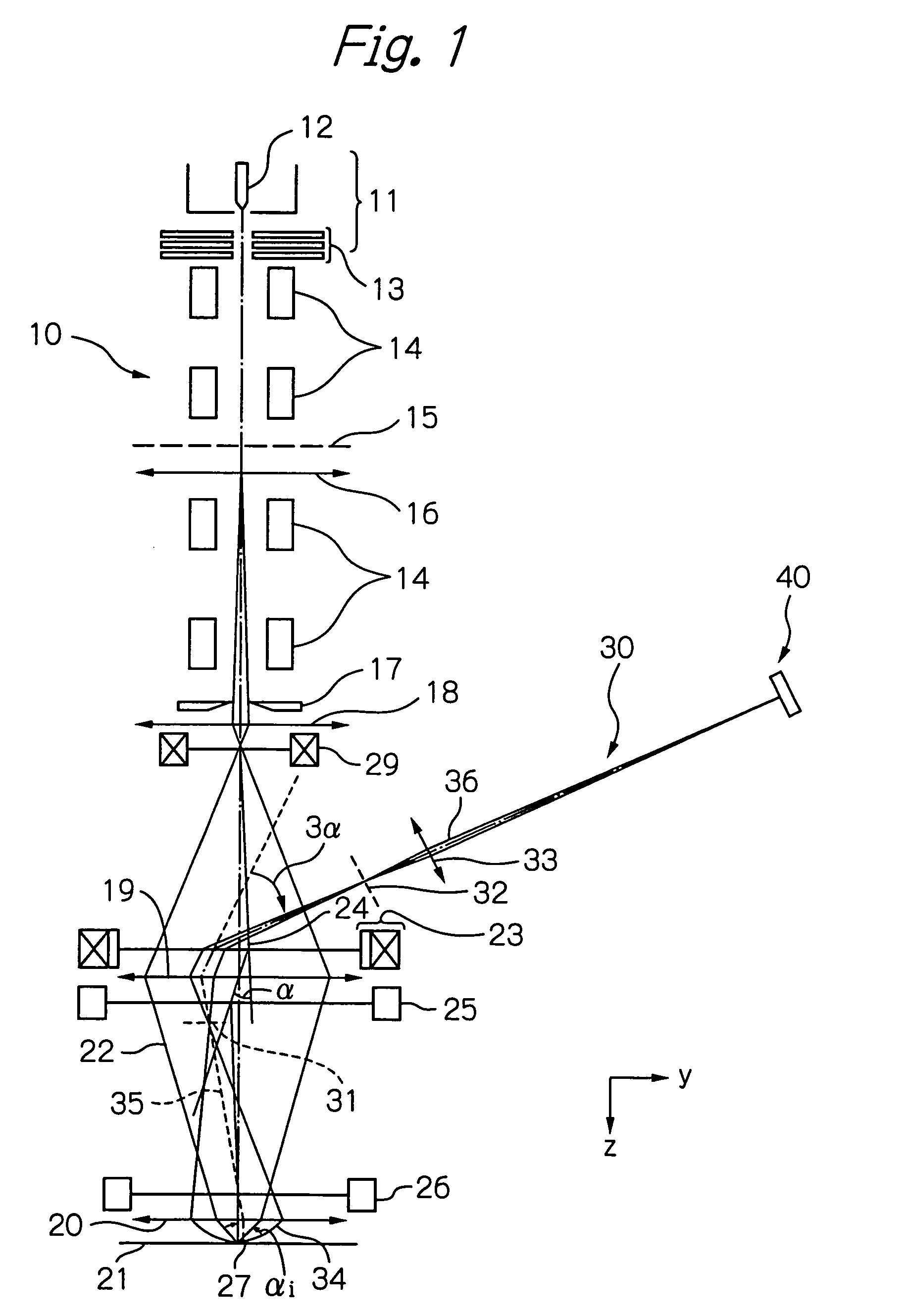
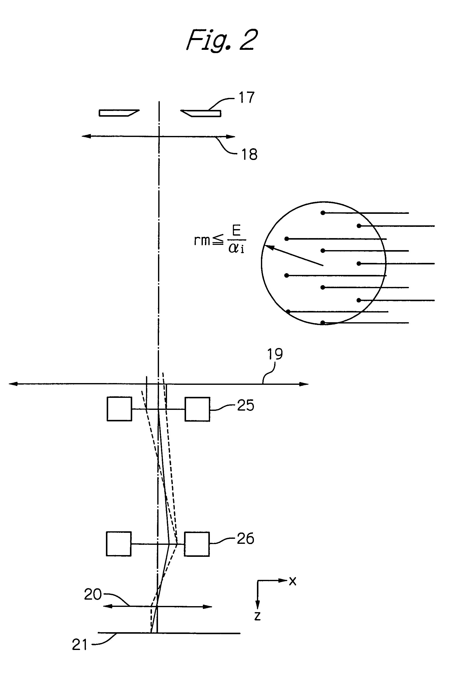
[0065]FIG. 1 shows an electron optical system in one embodiment of the present invention, comprising a primary optical system 10, a secondary optical system 30 and a detecting system 40.

[0066]In the primary optical system, an electron gun 11 controlls a LaB6 cathode 12 to be operative under a space-charge limited condition to thereby reduce a shot noise. An anode 13 is composed of three sheets of electrodes, and it can be controlled to perform a lens operation as well as to produce a high intensity condition and / or a high emittance condition by changing a voltage applied to a first anode. An axial alignment with this anode may be accomplished by shifting the cathode and the Wehnelt mechanically in the XY directions or the θ direction. Further, the axial alignment of the beam emitted from the electron gun is carried out by axial-aligning deflectors 14. A multi-aperture plate 15 is disposed in a certain range of the beam diverged from the electron gun 11, for example, within a range o...

second embodiment

[0078]An embodiment of a pattern evaluation method according to the present invention will now be described.

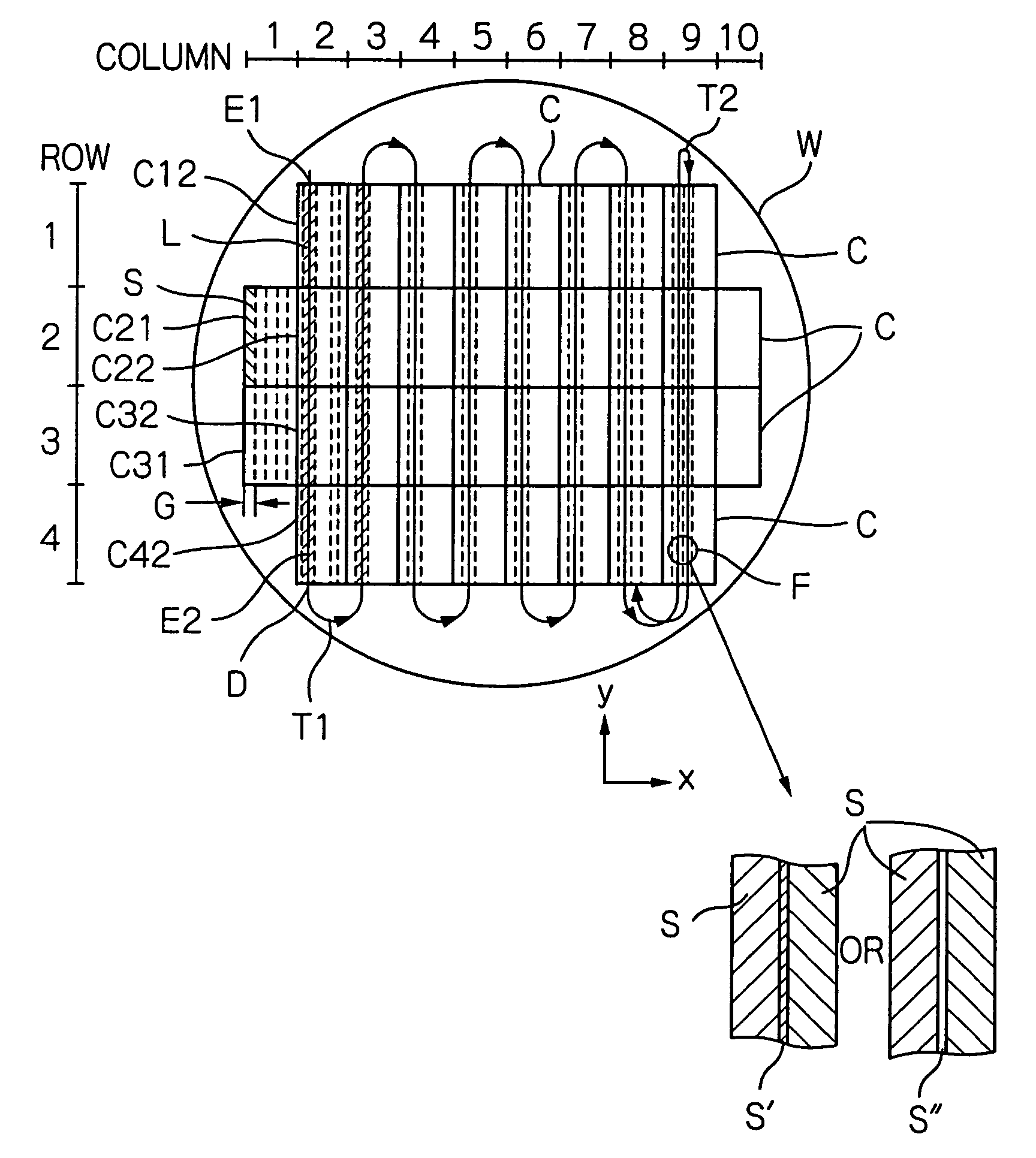
[0079]FIG. 3(a) is a plan view illustrating a way for dividing a chip, or a sample, formed on a wafer into stripes and FIG. 3(b) is an enlarged view of a part designated by “F” in FIG. 3(a). Further, FIG. 4 is an enlarged plan view illustrating a way for dividing the chip into stripes.

[0080]In FIG. 3(a), the Z axis is taken in parallel to a normal line of a surface (the drawing sheet surface) of a wafer W, the X axis is taken in parallel to the sheet surface in the left and right direction, and the Y axis is taken in parallel to the sheet surface in the up and down direction. In this illustrated embodiment, a large number of chips C are formed on the wafer W almost across an entire surface thereof by 10 columns in the X direction and 4 or 2 rows in the Y direction. To simplify the description, in the drawings, a row address (1 to 4) is assigned along a longitudinal direction a...

third embodiment

[0113]FIG. 8 is a flow chart representing a way for applying the electron beam apparatuses or the pattern evaluation methods, which have been described in the above embodiments, to the evaluation of a wafer in a semiconductor device manufacturing process.

[0114]An example of the device manufacturing process will now be described with reference to a flow chart of FIG. 8.

[0115]The manufacturing process includes the following main processes.

[0116](1) A wafer manufacturing process for manufacturing a wafer (or wafer preparing process for preparing a wafer). (Step 10)

[0117](2) A mask manufacturing process for fabricating a mask to be used in the exposure (or a mask preparing process). (Step 11)

[0118](3) A wafer processing process for performing any processing treatments necessary for the wafer. (Step 12)

[0119](4) A chip assembling process for cutting out those chips formed on the wafer one by one to make them operative. (Step 13)

[0120](5) A chip inspection process for inspecting an assemb...


PUM

PropertyMeasurementUnit
widthaaaaaaaaaa
widthaaaaaaaaaa
sizeaaaaaaaaaa

Abstract

Provided is an electron beam apparatus in which an electron beam emitted from an electron gun is separated by a plurality of apertures, images of said apertures are reduced in more than two stages to form multi-beams on a sample surface and to scan said sample thereby, and secondary electrons from said sample are passed through an objective lens, where distances between said secondary electrons are extended, further through an E×B separator, where said secondary electrons are separated from the primary beam, and finally onto secondary electron detectors, where said secondary electrons are detected, wherein a lens defined in the second step for reducing said image of the aperture is composed of two stage lens and an enlarged image of the secondary electron is formed on a position between a first and a second lenses of said two stage lens, thereby reducing an aberration of the optical system for detecting the secondary electrons and allowing as many multi-beams as possible to be formed in the vicinity of a single optical axis.

Description

BACKGROUND OF THE INVENTION[0001]The present invention relates to an apparatus providing a pattern evaluation of a sample, for example, a substrate having a pattern with a minimum line width not greater than 0.1 μm with a high throughput, and also to an evaluation method of a pattern by using the same apparatus.[0002]The present invention further relates to a pattern evaluation method that provides an evaluation, such as a defect inspection for a chip having a pattern with a minimum line width not greater than 0.1 μm in an inexpensive manner, with a reduced foot print as well as with a high throughput.[0003]The present invention further relates to a method for manufacturing a device by using said electron beam apparatus or pattern evaluation method.[0004]In the evaluation of a pattern formed on a substrate by using an electron beam, it has been conventionally suggested to use a multi-beam in order to improve the throughput. Such suggestions may be categorized roughly into two method...

Claims


Application Information

Patent Timeline
Patent Type & Authority Patents(United States)
IPC IPC(8): H01J37/28G01N23/00G01N23/225
CPCG01N23/2251H01J2237/2446H01J2237/1534H01J2237/0492
Inventor NAKASUJI, MAMORUKATO, TAKAOKIMBA, TOSHIFUMISATAKE, TOHRU
Owner EBARA CORP
Learn More