
Solid state lighting device with reduced form factor including LED with directional emission and package with microoptics

a solid-state lighting and directional emission technology, applied in the field of semiconductor devices, can solve the problems of large external optics and the suffering of conventional led arrays used for lighting applications

Inactive Publication Date: 2006-02-14
GENERAL ELECTRIC CO
View PDF32 Cites 57 Cited by
  • Summary
  • Abstract
  • Description
  • Claims
  • Application Information

AI Technical Summary

Problems solved by technology

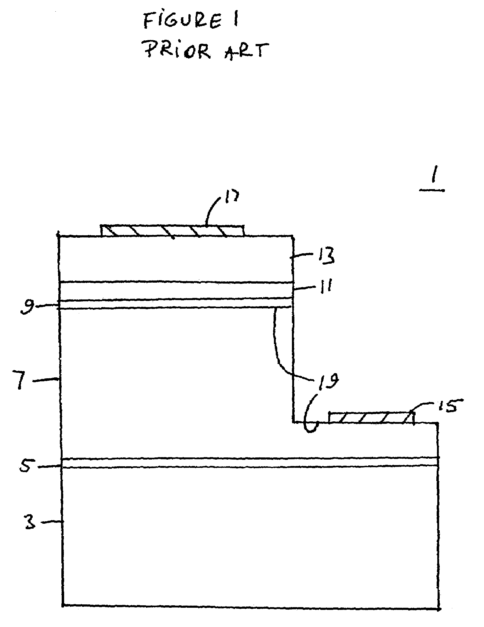
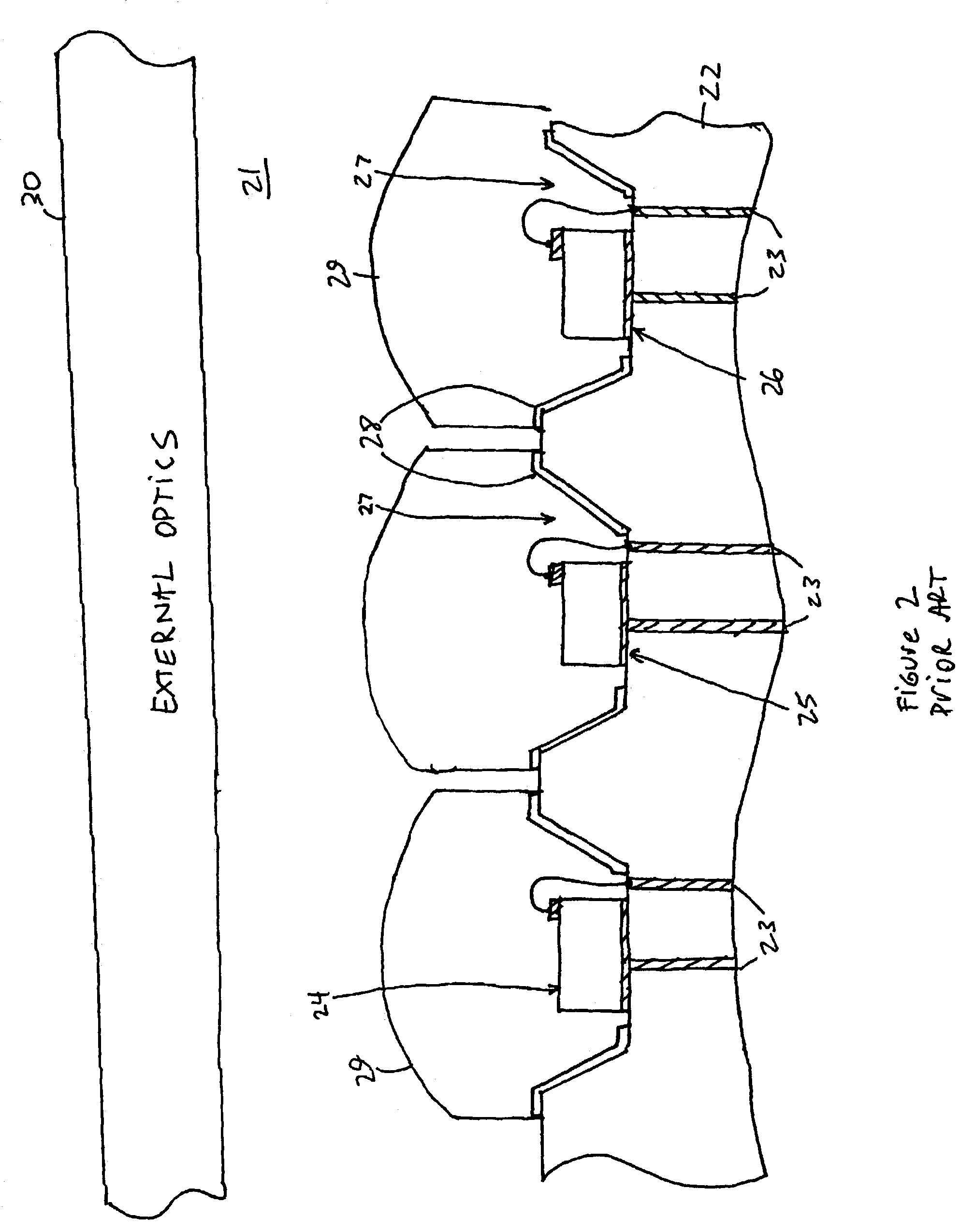
However, the conventional LED arrays used for lighting applications suffer from several disadvantages.
However, the external optics are relatively large.
Therefore, the individual LEDs in the array have to be spaced apart at an undesirably large distance in order for the external optics to work properly.

Method used


Image

  • Solid state lighting device with reduced form factor including LED with directional emission and package with microoptics
  • Solid state lighting device with reduced form factor including LED with directional emission and package with microoptics
  • Solid state lighting device with reduced form factor including LED with directional emission and package with microoptics

Examples


Embodiment Construction

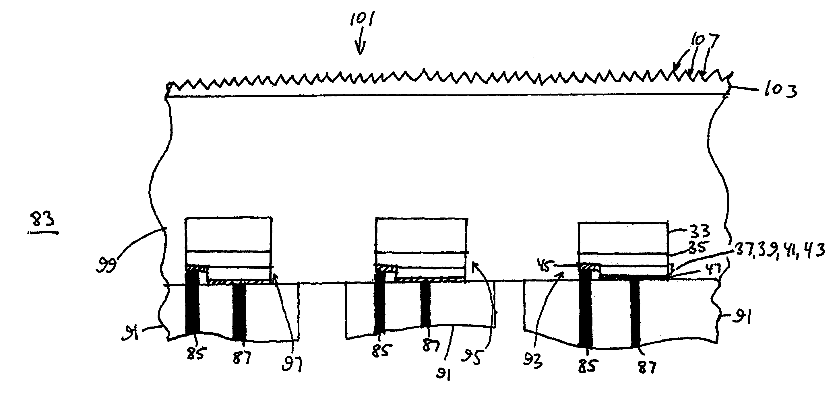
[0035]In view of the problems in the prior art, it is desirable to obtain an LED array with a lower form factor without sacrificing the light extraction efficiency and / or the color mixing. The present inventors have discovered that the reflector cavity and the dome lens may be omitted without substantially lowering the light extraction efficiency if a directional emission LED is used in the light emitting device. Preferably, the directional emission LED is a lateral current injection, resonant cavity LED. Furthermore, the lower form factor may be achieved while still retaining the color mixing ability by integrating color mixing microoptical elements directly into the LED package.

A. The Resonant Cavity LED of the First Preferred Embodiment

[0036]Resonant cavity LEDs (“RCLEDs”, also known as microcavity LEDs) are described in U.S. Pat. Nos. 5,226,053 and 5,779,924, which are incorporated herein by reference. However, these RCLEDs are vertical current injection RCLEDs and thus have one...


PUM


Abstract

A light emitting device containing an array of directional emission LEDs is provided. The directional emission LEDs of the array may be substrate emitting, lateral current injection, resonant cavity LEDs mounted in a flip-chip configuration. Each LED may emit a different color of light, such that the output of the array appears white to an observer. The LED array package may contain microoptical elements, such as a diffraction grating or microprisms, integrated into the light emitting surface of the package. The microoptical elements are used to mix the light beams emitted by individual LEDs in the array.

Description

[0001]This is a Divisional Application of application Ser. No. 09 / 686,910, filed Oct. 12, 2000, now abandoned, incorporated herein by reference.BACKGROUND OF THE INVENTION[0002]This invention relates generally to a semiconductor device and specifically to a directional emission light emitting diode (“LED”) array with microoptic elements.[0003]Semiconductor light emitting diodes are semiconductor chips that are mounted in a package and emit radiation in response to an applied voltage or current. These LEDs are used in a number of commercial applications such as automotive, display, safety / emergency and directed area lighting. A high brightness is desired for these applications.[0004]White light emitting LED arrays are made by placing a plurality of LEDs into a package, where the individual LEDs emit different color lights. For example, by including red, green and blue emitting LEDs into an array, their combined output appears white to a human observer. Other LED arrays contain LEDs w...

Claims


Application Information

Patent Timeline
Patent Type & Authority Patents(United States)
IPC IPC(8): H01L21/56H01L25/075H01L33/10H01L33/40H01L33/46H01L33/54
CPCH01L33/46H01L33/105H01L25/0753H01L2924/12041H01L33/405H01L33/54H01L2224/32225H01L2224/48091H01L2224/48235H01L2224/73265H01L2924/01012H01L2924/01079H01L2933/0091H01L2924/00014
Inventor TASKAR, NIKHIL RAMESHKRISHNAMURTHY, VIKRAM BIDARE
Owner GENERAL ELECTRIC CO
Learn More