Shared delay circuit of a semiconductor device
a semiconductor device and delay circuit technology, applied in pulse manipulation, pulse technique, instruments, etc., can solve the problems of presenting different time delay characteristics and deteriorating area efficiency
- Summary
- Abstract
- Description
- Claims
- Application Information
AI Technical Summary
Benefits of technology
Problems solved by technology
Method used
Image
Examples
Embodiment Construction
[0028]Hereinafter, a preferred embodiment of the present invention will be described with reference to the accompanying drawings. In the following description and drawings, the same reference numerals are used to designate the same or similar components, and so repetition of the description on the same or similar components will be omitted.
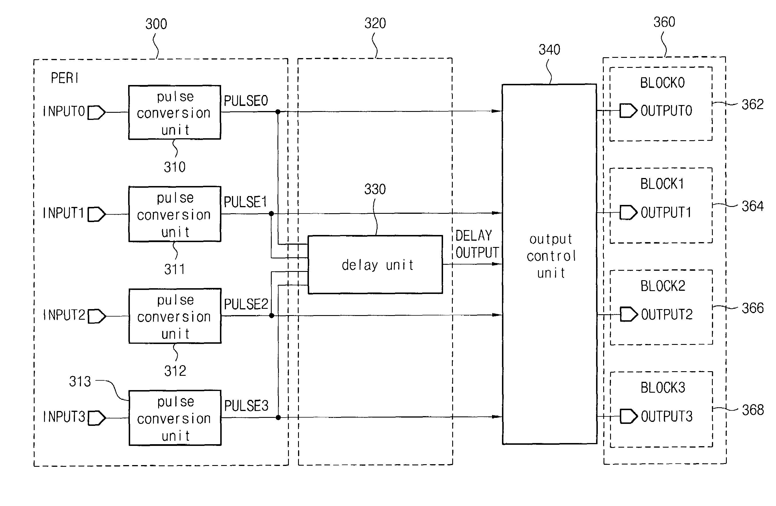
[0029]FIG. 3 is a circuit diagram of a shared delay circuit of a semiconductor device according to an embodiment of the present invention.
[0030]As shown in FIG. 3, the shared delay circuit of a semiconductor device according to the present invention includes an input signal conversion unit 300, a shared delay unit 320, and an output control unit 340. A circuit block unit 360 is a part which receives and uses the output signals of the output control unit 340.
[0031]In FIG. 3, the input signal conversion unit 300 is composed of a plurality of pulse conversion units 310, 311, 312 and 313 corresponding to a plurality of input signals INPUT 0, INPUT 1, ...
PUM
 Abstract
Description
Claims
Application Information
 - R&D
- Intellectual Property
- Life Sciences
- Materials
- Tech Scout
- Unparalleled Data Quality
- Higher Quality Content
- 60% Fewer Hallucinations
Browse by: Latest US Patents, China's latest patents, Technical Efficacy Thesaurus, Application Domain, Technology Topic, Popular Technical Reports.
© 2025 PatSnap. All rights reserved.Legal|Privacy policy|Modern Slavery Act Transparency Statement|Sitemap|About US| Contact US: help@patsnap.com


