
Memory device with improved output operation margin

a memory device and output operation technology, applied in the field of memory devices with improved output operation margin, can solve the problems of insufficient speed of sdr memory devices to meet the speed requirement of high-speed systems, inability to perform process within the memory devices, and inability to use data access methods employed in conventional synchronous memory devices. achieve the effect of improving operation margin, high frequency and stable operation

Inactive Publication Date: 2006-01-17
SK HYNIX INC
View PDF15 Cites 52 Cited by
  • Summary
  • Abstract
  • Description
  • Claims
  • Application Information

AI Technical Summary

Benefits of technology

[0033]It is, therefore, an object of the present invention to provide a synchronous memory device, which is capable of providing wide-ranging CAS latency modes and stably operating at high frequency because of an improved operation margin.

Problems solved by technology

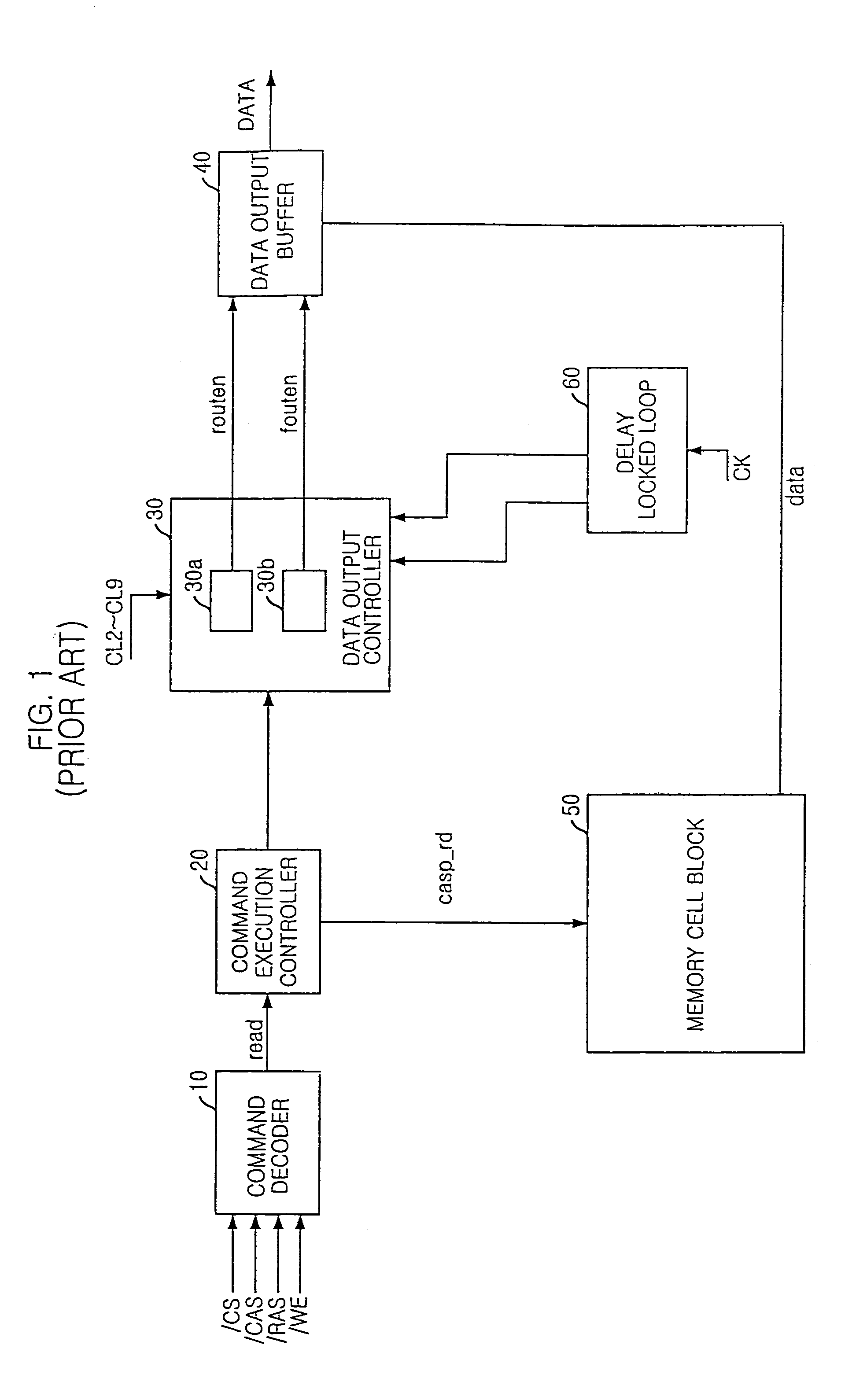
However, such an SDR memory device is insufficient to satisfy a speed requirement in a high-speed system.
However, since the DDR memory device must input / output two data for one clock cycle, data access method employed in the conventional synchronous memory device cannot be used any more.
However, it is difficult to perform the process within the memory device.
Accordingly, when the memory device operates in the wide CAS latency mode ranging from 2 to 9, the operation margin of the data output controller is decreased, thus making it impossible to operate the memory device at a high frequency.

Method used


Image

  • Memory device with improved output operation margin
  • Memory device with improved output operation margin
  • Memory device with improved output operation margin

Examples


Embodiment Construction

[0045]Hereinafter, the present invention will be described in detail with reference to the accompanying drawings.

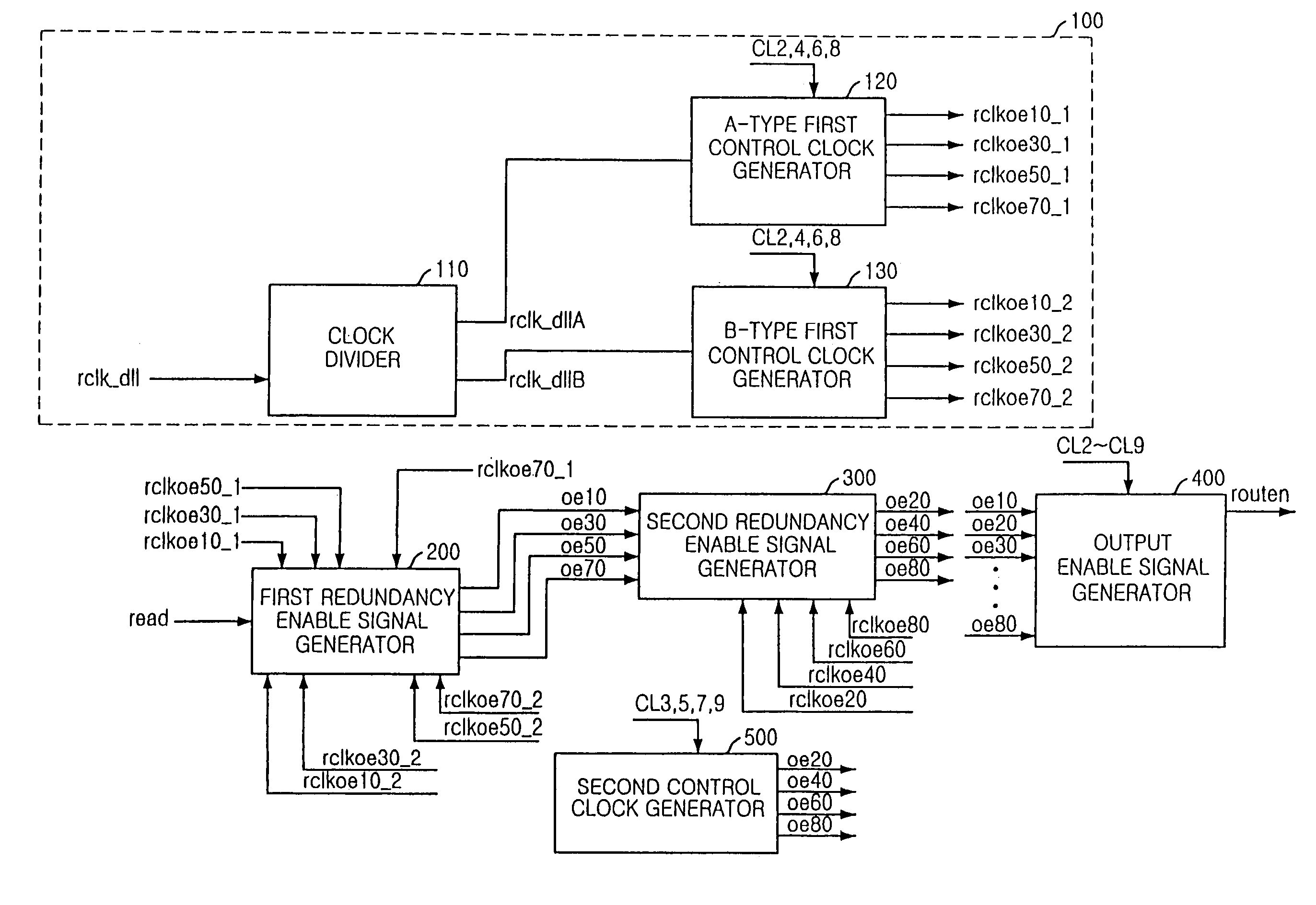
[0046]FIG. 4 is a block diagram illustrating a data output controller of a memory device in accordance with one embodiment of the present invention.

[0047]Referring to FIG. 4, a data output controller of a memory device in accordance with an embodiment of the present invention includes a control clock generator 100, a first redundancy enable signal generator 200, a second redundancy enable signal generator 300, and an output enable signal generator 400.

[0048]The control clock generator 100 generates an A-type first control clock rclk—dllA and a B-type first control clock rclk—dllB in order to output a data output enable signal routen according to a selected CAS latency mode (CL=2 to CL=9). The A-type first control clock rclk—dllA is a clock that is supplied by dividing DLL clock signal rclk—dll by two and the B-type first control clock rclk—dllB is an inverted A-type first...


PUM


Abstract

A synchronous memory device which generates a data output enable signal corresponding to a set CAS latency mode including: a control clock generator for generating an A-type first control clock and a B-type first control clock; a first redundancy enable signal generator for shifting an internal read signal by a predetermined interval in synchronization with one of the A-type first control clock and the B-type first control clock and generating a plurality of first redundancy enable signals; a second redundancy enable signal generator for synchronizing the plurality of first redundancy enable signals with a DLL clock and generating a plurality of second redundancy enable signals; and an output enable signal generator for selecting one redundancy enable signal corresponding to the set CAS latency mode among the first redundancy enable signals and the second redundancy enable signals and generating the selected redundancy enable signal as the data output enable signal.

Description

FIELD OF THE INVENTION[0001]The present invention relates to a semiconductor memory device; and, more particularly, to a data output control circuit for controlling data output in memory device.DESCRIPTION OF RELATED ART[0002]Developments on semiconductor memory devices have been kept on in order to obtain high integration and improved operating speed. Synchronous memory devices operating in synchronization with external clock have been introduced to improve the operating speed.[0003]Among the synchronous memory devices, a single data rate (SDR) memory device inputs / outputs one data through one data pin for one clock cycle in synchronization with rising edges of an external clock.[0004]However, such an SDR memory device is insufficient to satisfy a speed requirement in a high-speed system. Accordingly, a double data rate (DDR) memory device that processes two data for one clock cycle has been proposed.[0005]The DDR memory device inputs / outputs two consecutive data through input / outp...

Claims


Application Information

Patent Timeline
Patent Type & Authority Patents(United States)
IPC IPC(8): G11C8/00G11C11/40
CPCG11C29/842G11C11/40
Inventor KIM, SI-HONGYOON, YOUNG-JIN
Owner SK HYNIX INC
Learn More