Image processing device for carrying out dodging treatment

a processing device and image technology, applied in the field of image filter circuits, can solve the problems of large difference, inability to perfectly reproduce images recorded on films or the like, and inability to fix the recording conditions under which images are recorded on films, etc., and achieve the effect of simple circuit arrangement and small siz

Inactive Publication Date: 2006-01-17
FUJIFILM CORP
View PDF11 Cites 4 Cited by
  • Summary
  • Abstract
  • Description
  • Claims
  • Application Information

AI Technical Summary

Benefits of technology

[0019]In view of the problem of prior art, an object of the present invention is to provide an image filter circuit which is small in size and has a simple circuit arrangement to obtain the dodging effect (the effect similar to that obtained by the dodging treatment which uses the areal exposure).

Problems solved by technology

In the prints made by the conventional direct exposure, the images recorded on a film or the like cannot be perfectly reproduced in some points such as resolution, color / density reproducibility and the like.
Incidentally, recording conditions under which an image is recorded on a film are not fixed and there are many cases where a large amount of difference exists between a bright portion and a dark portion as found in an image recorded using an electronic flash, a backlighted scene and the like.
When such a film image is exposed by a conventional method and made to a finished print, there is a tendency that details become imperceptible due to insufficient gradation in either one of a bright portion and a dark portion on the print.
Thus, a problem arises in that an image filter circuit for carrying out filter treatment is increased in size.

Method used


Image

  • Image processing device for carrying out dodging treatment
  • Image processing device for carrying out dodging treatment
  • Image processing device for carrying out dodging treatment

Examples


Embodiment Construction

[0031]An embodiment of an image filter circuit of the present invention will be described below with reference to accompanying drawings.

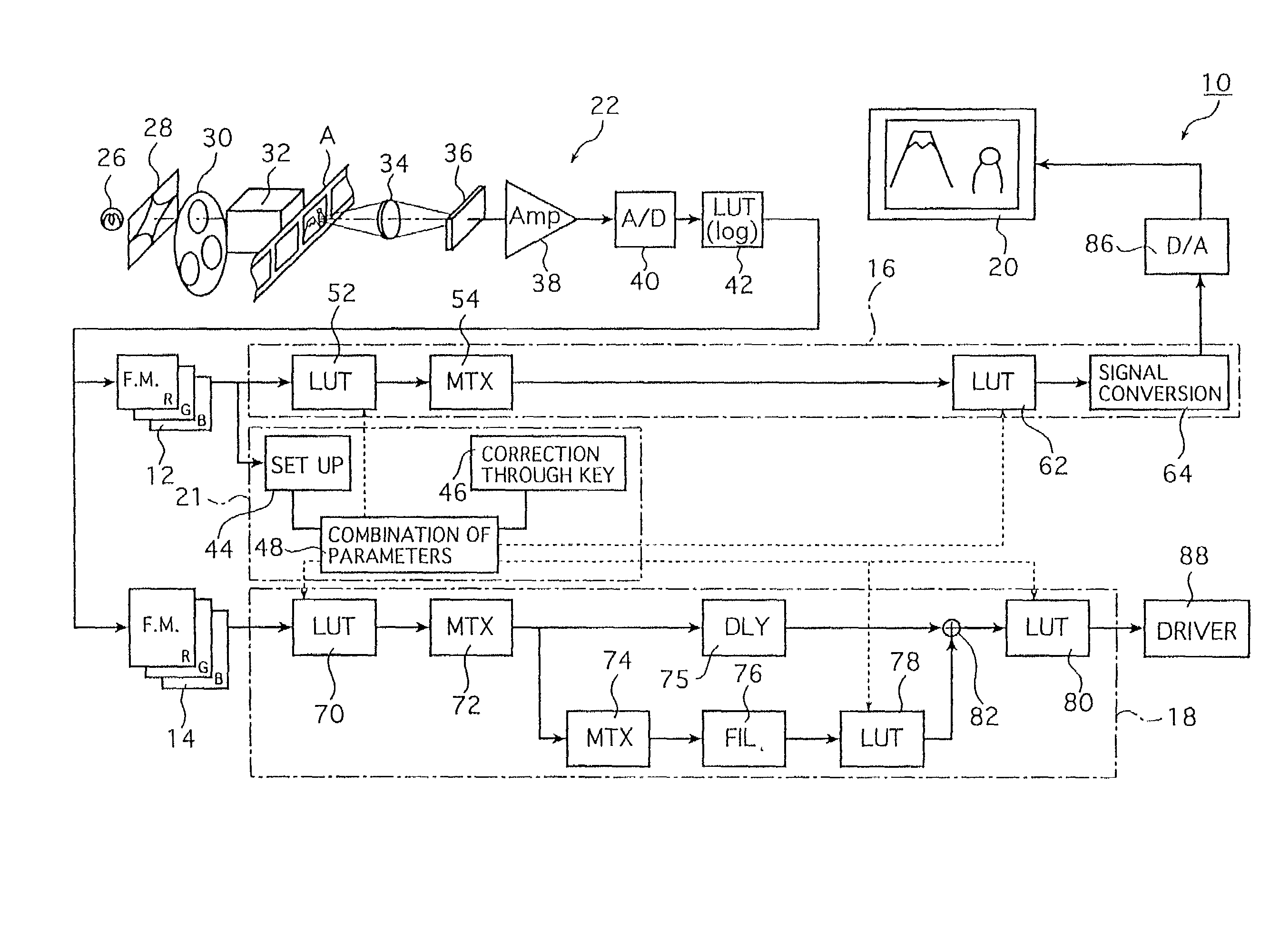
[0032]FIG. 1 shows a schematic view of an embodiment of an image processing apparatus making use of the image filter circuit of the present invention. An image processing apparatus 10 shown in FIG. 1 processes input image signals read out by an image reading apparatus (hereinafter, referred to as a reading apparatus) 22 and outputs the thus processed input image signals to an image recording apparatus (hereinafter, referred to as a recording apparatus) as output image signals in accordance with a recorded image. A digital photo printer is composed of the reading apparatus 22, the image processing apparatus 10 and the recording apparatus and the like.

[0033]The reading apparatus 22 reads out photoelectrically an image recorded on a film A and supplies it to the processing apparatus 10. The reading apparatus includes a light source 26, a variable diaph...


PUM


Abstract

An image filter circuit generates unsharp image signals to subject image signals to a dodging treatment which adjusts areas of exposure over an entire image within an image processing apparatus for image processing the image signals. The circuit includes an IIR type filter for carrying out a filtering treatment to generate the unsharp image signals. It further includes a FIFO type field memory for delaying image signals which are not subjected to the filtering treatment at the hR filter for a time corresponding to the delay time of image signals which have been subjected to the filtering treatment at the IIR type filter. The image filter circuit, which obtains the unsharp image signals corresponding to an unsharp mask for obtaining a dodging effect, can be made small in size with a simplified circuit arrangement.

Description

[0001]This application is a divisional of Application No. 08 / 873,463, filed on Jun. 12, 1997, now U.S. Pat. No. 6,256,424, the entire contents of which are hereby incorporated by reference.BACKGROUND OF THE INVENTION[0002]1. Field of the Invention[0003]The present invention relates to an image filter circuit for generating unsharp image signals used to subject image signals to dodging treatment in an image processing apparatus for image processing the image signals.[0004]2. Description of the Related Art[0005]At present, an image recorded on a photographic film such as a negative film, a reversal film and the like (hereinafter referred to as a film) is printed to a photosensitive material such as a photographic paper and the like by so-called direct exposure in which the photosensitive material is subjected to areal exposure by being projected with an image recorded on a film.[0006]Recently, research of printers making use of digital exposure, that is, digital photo printers has bee...

Claims


Application Information

Patent Timeline
Patent Type & Authority Patents(United States)
IPC IPC(8): G06K15/00H04N1/40G03B27/32G06T5/20G06T5/40H04N1/409H04N5/262
CPCH04N1/409G06T5/008
Inventor MURAKAMI, HIROSHI
Owner FUJIFILM CORP
Why Eureka
Try Eureka