
N type impurity doping using implantation of P2+ ions or As2+ Ions

a technology of implantation beam and impurity, which is applied in the direction of basic electric elements, electrical equipment, semiconductor devices, etc., can solve the problems of reducing throughput rates, less than 10 kev, and ion beam energy must be reduced, so as to increase beam energy, increase beam energy, and increase beam energy

Inactive Publication Date: 2006-01-03
TAIWAN SEMICON MFG CO LTD
View PDF3 Cites 5 Cited by
  • Summary
  • Abstract
  • Description
  • Claims
  • Application Information

AI Technical Summary

Benefits of technology

[0009]It is another principle objective of this invention to provide a method of implanting arsenic in source / drain regions using ion beam implantation with increased beam energy in applications having very shallow junctions.

Problems solved by technology

One problem encountered as device geometries become smaller and source / drain junction depths become smaller is that the ion beam energy must become lower, in some cases less than 10 KeV.
At these low energies it is difficult to obtain sufficient ion beam density resulting in lower throughput rates and increased implant cycle times, which directly impact cost.

Method used


Image

  • N type impurity doping using implantation of P2+ ions or As2+ Ions
  • N type impurity doping using implantation of P2+ ions or As2+ Ions
  • N type impurity doping using implantation of P2+ ions or As2+ Ions

Examples


Embodiment Construction

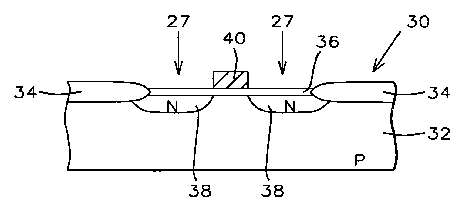
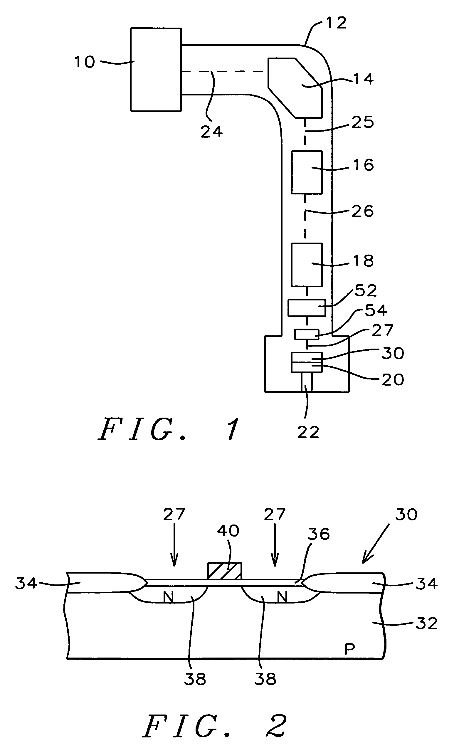
[0017]The preferred embodiments of this invention will now be described with reference to FIGS. 1–4. FIG. 1 shows a schematic view of an ion beam apparatus. Different ion beam systems may differ from the one shown and described herein but certain key features will be common to all ion beam systems. The ion beam apparatus has an ion source 10 which uses a small accelerating voltage to inject an ion beam 24 into an evacuated enclosure 12. Ion sources can be solid materials or gasses such as solid phosphorous, phosphine gas, solid arsenic, or SDS arsine.

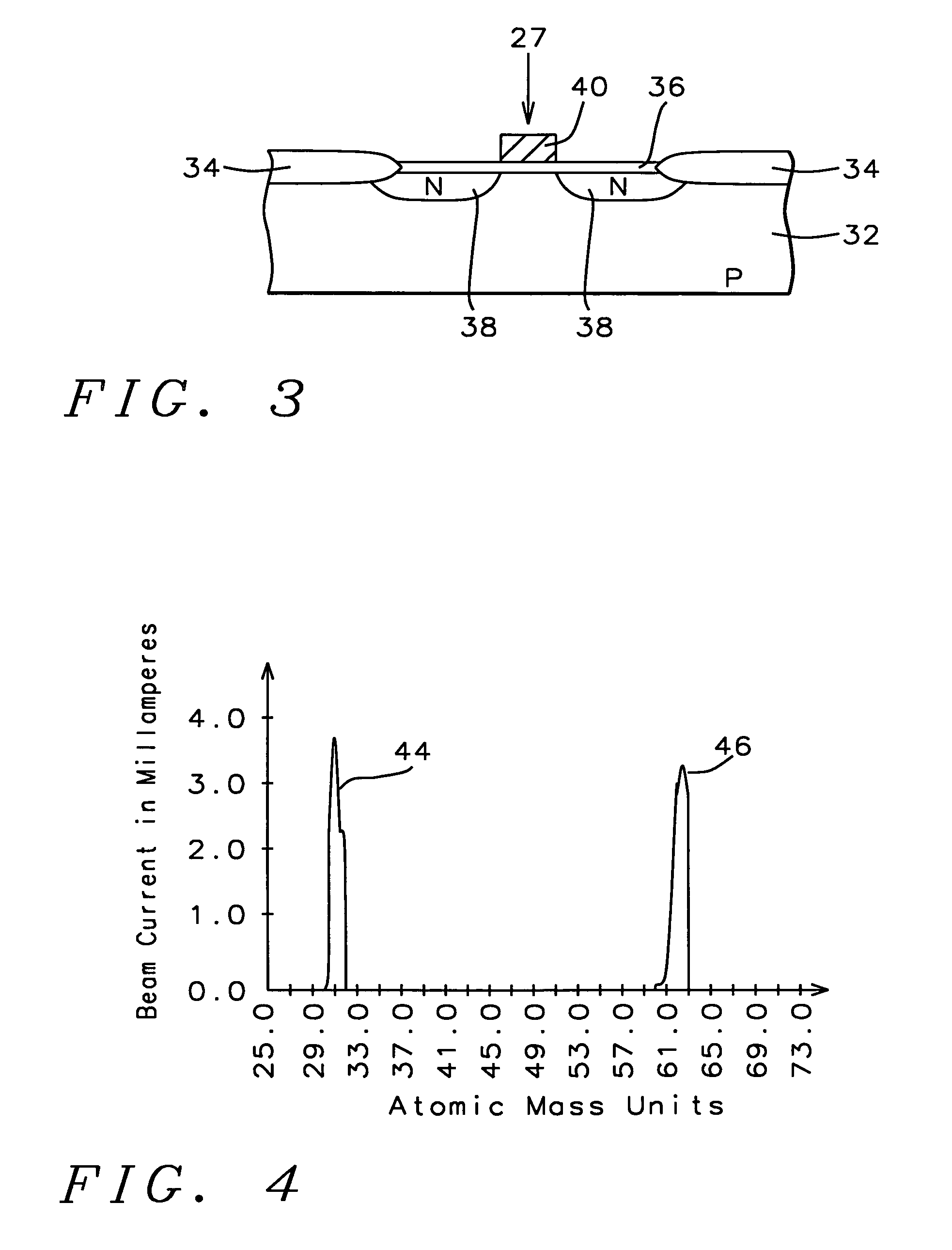
[0018]Referring again to FIG. 1, the beam then enters a magnetic analyzer 14 which is selected to select particles with a particular mass to charge ratio for the beam 25 exiting the magnetic analyzer. For the example of an ion source 10 using solid phosphorous or phosphine gas the magnetic analyzer 14 is adjusted to select singly charged P2 ions which have a mass of 62 atomic mass units and a charge equal to the charge of a single elect...


PUM


Abstract

A method for using ion implantation to implant phosphorous or arsenic impurities into shallow source / drain regions or into polysilicon electrodes used in devices having shallow source / drain electrodes. A phosphorous source having an abundance of P2+ ions is used in an ion beam system adjusted to select P2+ ions. Since each ion contains two phosphorous atoms the ion beam requires twice the beam energy and half the beam density. This provides good wafer throughput and improved source life. An arsenic source having an abundance of As2+ ions can be substituted for the solid phosphorous source resulting in a beam of As2+ ions.

Description

BACKGROUND OF THE INVENTION[0001](1) Field of the Invention[0002]This invention relates to the use of an ion implantation beam of P2+ ions or As2+ ions to dope N type shallow junction source / drain regions or gate electrodes used in devices with shallow source / drain regions. Use of the P2+ ions or As2+ ions uses lower ion density and higher beam energy resulting in improved throughput and ion source life.[0003](2) Description of the Related Art[0004]As junctions become very shallow the use of P+ ion beams or As+ ion beams becomes a problem because beam energies must be kept very low while the beam ion densities must be kept very high. These requirements leads to reduced ion source life and reduced wafer throughput. This invention overcomes this problem using P2+ ion beams or As2+ ion beams.[0005]U.S. Pat. No. 5,155,369 to Current describes a method of using two doses of ions in an ion beam to provide implantation for shallow junction devices. A first dose of ions is implanted to prod...

Claims


Application Information

Patent Timeline
IPC IPC(8): H01L21/425H01L21/265H01L21/28H01L21/336
CPCH01L21/2652H01L29/66575H01L21/28035H01L21/2658
Inventor LEE, BUAN HENGLOW, TECK HONGWANG, HAI RONGYING, TANGLAM, ZADIG CHERNG-CHING
Owner TAIWAN SEMICON MFG CO LTD
Learn More