Optical modules and methods of making the optical modules

Inactive Publication Date: 2005-12-27
OPNEXT JAPAN INC
View PDF8 Cites 6 Cited by
  • Summary
  • Abstract
  • Description
  • Claims
  • Application Information

AI Technical Summary

Benefits of technology

[0009]More particularly, the higher the operating frequency, the more expensive the pulse pattern generator and the jitter analyzer, and it takes several minutes for the measurement, thus resulting in an increase of the adjustment cost.
[0011]It is an object of the present invention to decrease the adjustment cost in the manufacture of an optical module and thereby provide a less expensive optical module.
[0012]It is another object of the present invention to provide a jitter transfer bandwidth adjusting method for an optical module less expensively.

Problems solved by technology

More particularly, the higher the operating frequency, the more expensive the pulse pattern generator and the jitter analyzer, and it takes several minutes for the measurement, thus resulting in an increase of the adjustment cost.
Consequently, in a CDR IC of a high speed such as 2.5 Gbps or 10 Gbps, such a high-speed signal as 2.5 Gbps or 10 Gbps is not allowed to pass in a normal probe, so it is difficult to adjust the jitter transfer bandwidth, for example, by trimming a resistor in IC at the time of DC test for the IC, and it has so far been required to make the adjustment by using external resistor and capacitor after mounting the circuit board of module.

Method used


Image

  • Optical modules and methods of making the optical modules
  • Optical modules and methods of making the optical modules
  • Optical modules and methods of making the optical modules

Examples


Embodiment Construction

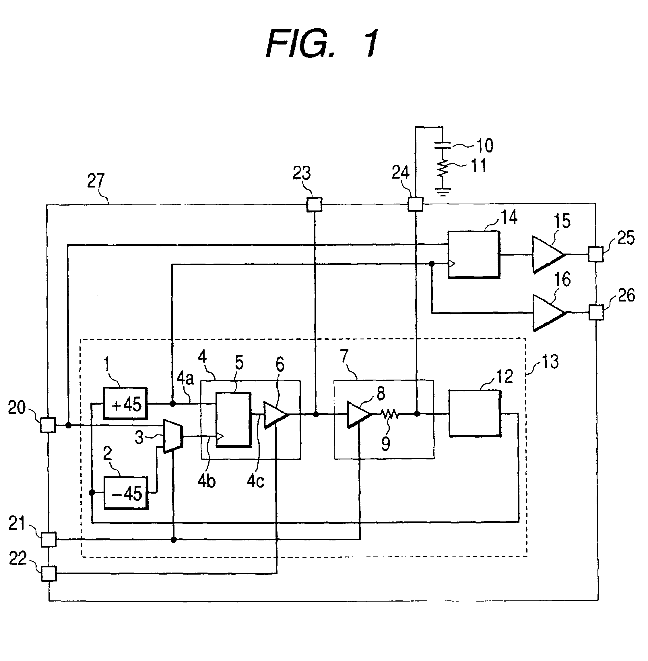
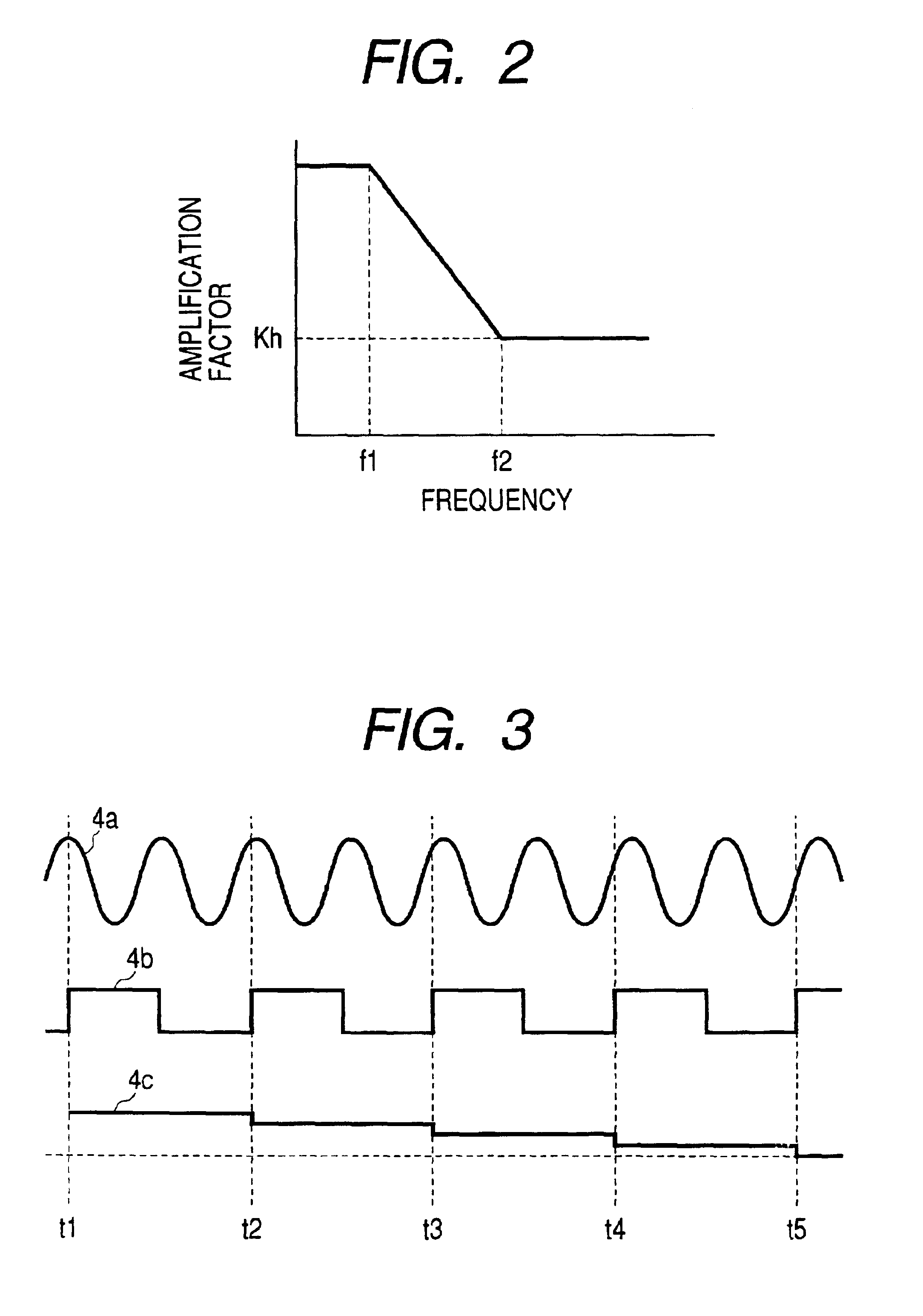
[0035]An optical module according to the present invention and a method of making the optical module, especially a jitter transfer bandwidth adjusting method, will be described below with reference to drawings.

[0036]First, an example of an optical communication system using the optical module according to the present invention will be described with reference to FIG. 11. In the same figure, an optical communication system comprises a multiplexer 60 for time-multiplexing a signal which has been subjected to a processing such as switching, a optical transmitter 61, an optical fiber for the transmission of a light signal outputted from the optical transmitter 61, a optical receiver 65 which receives a signal from the optical fiber 64 and converts it into an electric a signal and which reproduces a clock, and a demultiplexer 70 which separates a signal so as to facilitate a digital processing.

[0037]The optical transmitter 61, which receives a data signal 61a and a clock signal 61b from ...


PUM


Abstract

A sample & hold type phase detector is used in a CDR IC and, in jitter transfer bandwidth adjustment, VCO output waveforms 90° out of phase with each other can be inputted to the phase detector, whereby a jitter transfer bandwidth can be calculated by only the measurement of frequency and of a DC voltage and it is possible to make a jitter transfer bandwidth adjustment in DC test for IC.

Description

BACKGROUND OF THE INVENTION[0001]The present invention relates to optical modules and methods of making the optical modules, or electronic devices using the optical modules and optical communication systems using the optical modules.[0002]FIG. 13 is a configuration diagram showing a conventional optical module with a jitter transfer bandwidth being adjusted and FIG. 14 is a flow chart showing an example of procedure from assembly to shipment of the conventional optical module.[0003]As shown in FIG. 13, a optical receiver 65 has a PD or APD 66 for conversion from alight signal into an electric signal, a transimpedance amplifier 67 for current / voltage conversion, a voltage amplifier 68, and a CDR IC 27. The CDR IC 27 has a PLL 13 which comprises a phase detector 4, a filter circuit 7 and a VCO 12, a decision circuit 14, a data output buffer 15, and a clock output buffer 16.[0004]In adjusting a jitter bandwidth of the optical module (CDR IC 27), an output signal from a pulse pattern ge...

Claims


Application Information

Patent Timeline
IPC IPC(8): H01L31/107H03L7/085H03L7/091H01L31/10H04B10/07H04B10/2507H04B10/40H04B10/50H04B10/60H04L7/033
CPCH03L7/091H04L7/033
Inventor CHUJO, NORIOYAMAMOTO, KEIICHIOSAKI, AKIOHIRANO, KATSUNORINAKAO, TAKAYUKISHIMOTSU, TOMOAKIHASEGAWA, ATSUSHIAOKI, TETSUYAYAMASHITA, TAKESHI
Owner OPNEXT JAPAN INC
Why Eureka
Try Eureka