
Method of making an integrated electromechanical switch and tunable capacitor

a technology of tunable capacitors and electromechanical switches, which is applied in the direction of relays, generators/motors, television systems, etc., and can solve problems such as not being as significan

Inactive Publication Date: 2005-11-29
FOR NAT RES INITIATIVES
View PDF2 Cites 27 Cited by
  • Summary
  • Abstract
  • Description
  • Claims
  • Application Information

AI Technical Summary

Benefits of technology

"The present invention is about a low-cost microwave switch and tunable capacitor that can handle signals from DC to millimeter-wave frequencies. The switch and tunable capacitor are made using movable beams actuated by thermo-mechanical or electrostatic forces. The devices are fabricated directly on finished silicon-based integrated circuit wafers, such as CMOS, BiCMOS or bipolar wafers. The invention allows for reconfiguration capability, where the functions and operation characteristics of active circuits do not change as a result of the process sequence. The invention also allows for the switching-in or out of selected passive components to change the overall circuit configuration, making it a versatile solution for various applications."

Problems solved by technology

However, if the electromechanical switches, control circuitry for the switches, and conductive traces among which the electrical reconfiguration is done are fabricated on different substrates, such benefits would not be as significant.

Method used


Image

  • Method of making an integrated electromechanical switch and tunable capacitor
  • Method of making an integrated electromechanical switch and tunable capacitor
  • Method of making an integrated electromechanical switch and tunable capacitor

Examples


Embodiment Construction

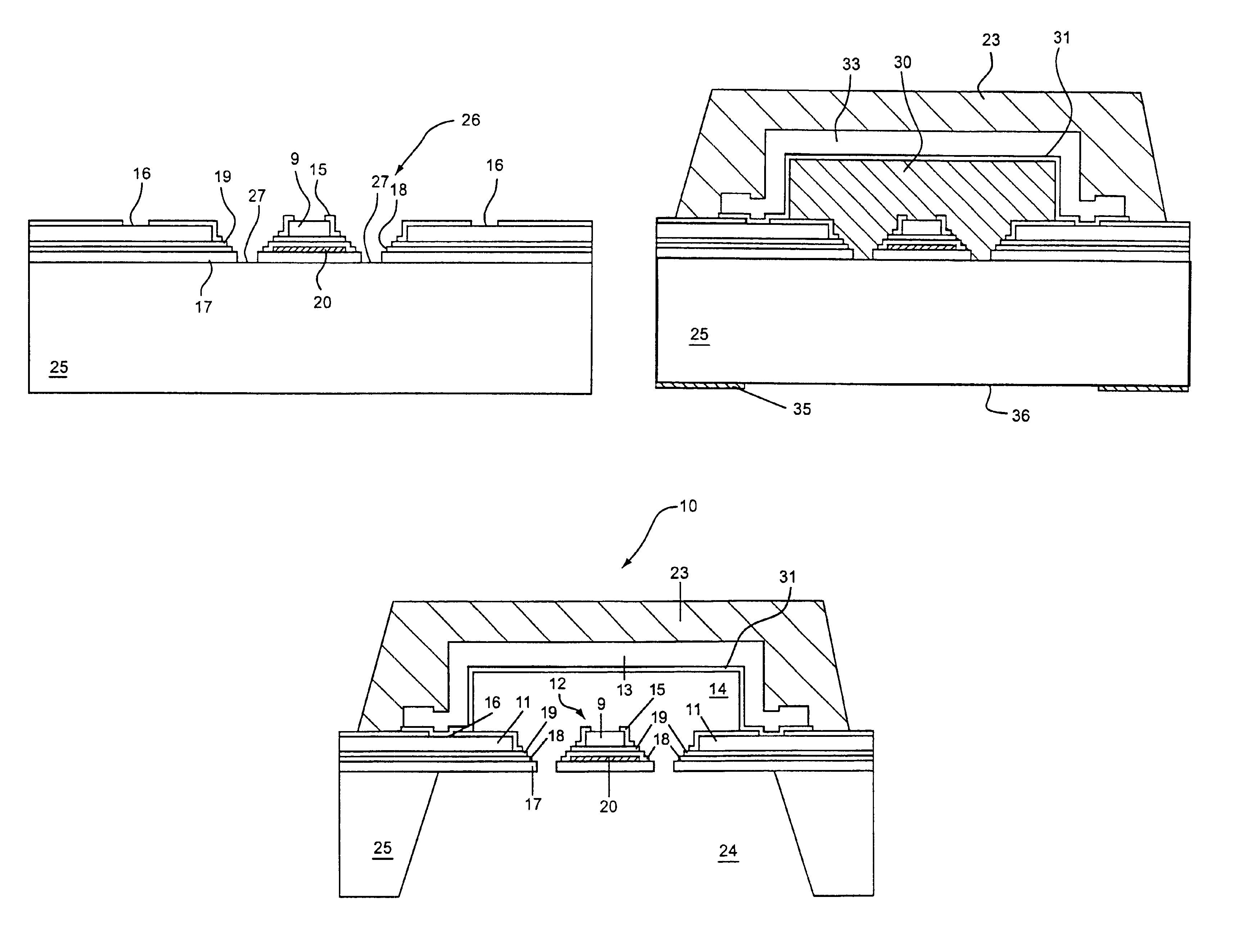
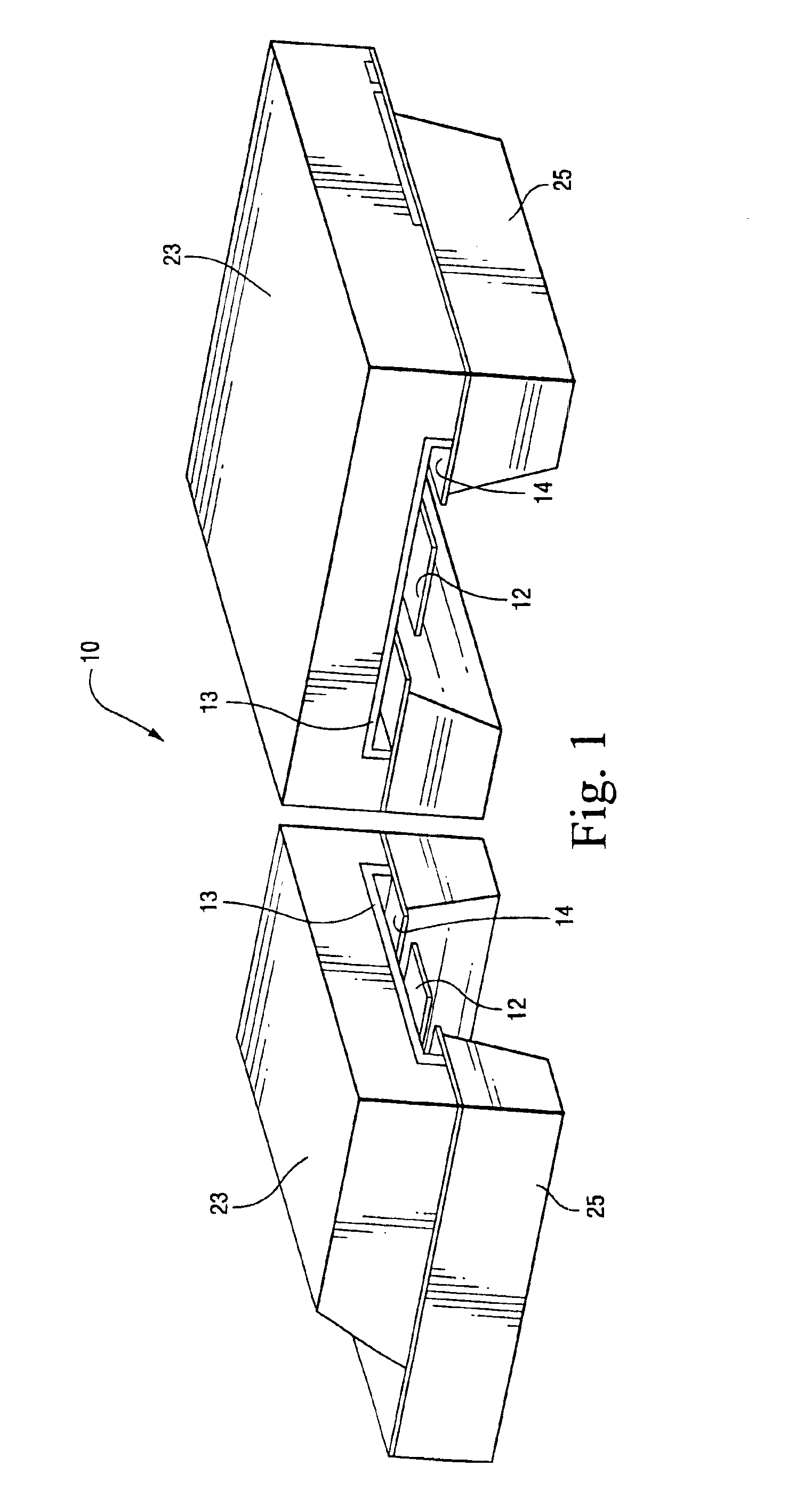
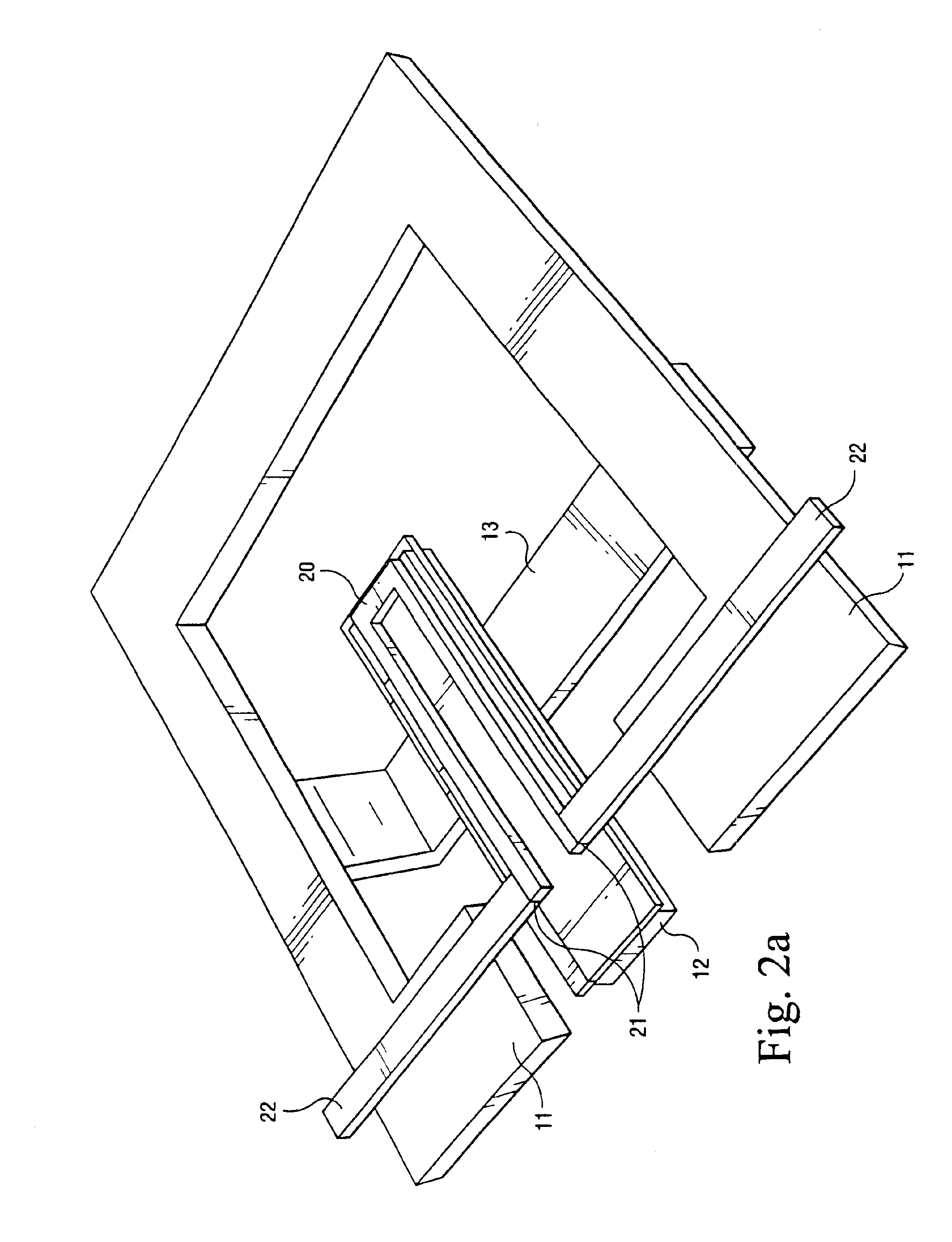
[0025]FIG. 1 is a perspective view of one embodiment of the electromechanical switch 10 of the present invention where switch 10 has been split open to show its internal construction. FIG. 4 is a top plan view of the electromechanical switch 10 in FIG. 1. FIG. 5 is a cross-sectional view of switch 10 taken along section line 5—5 shown in FIG. 4. Switch 10 is fabricated on a silicon wafer substrate 25, and includes a moveable beam 12 that moves within a cavity 14 to contact a conductive metal bridge 13. Deposited on top of substrate 25 is a superstrate 23 which supports conductive bridge 13. FIG. 2(a) is a bottom view of a thermally-actuated embodiment of switch 10, illustrated without the mechanical support layers, i.e., substrate 25 and superstrate 23, being shown for ease in understanding the operation of switch 10.

[0026]As shown in FIG. 2(a), switch 10 includes an n-shaped polysilicon heater 20 and two traces 22 that are formed in a first metal layer (not shown as before etching)...


PUM


Abstract

A monolithically integrated, electromechanical microwave switch, capable of handling signals from DC to millimeter-wave frequencies, and an integrated electromechanical tunable capacitor are described. Both electromechanical devices include movable beams actuated either by thermo-mechanical or by electrostatic forces. The devices are fabricated directly on finished silicon-based integrated circuit wafers, such as CMOS, BiCMOS or bipolar wafers. The movable beams are formed by selectively removing the supporting silicon underneath the thin films available in a silicon-based integrated circuit technology, which incorporates at least one polysilicon layer and two metallization layers. A cavity and a thick, low-loss metallization are used to form an electrode above the movable beam. A thick mechanical support layer is formed on regions where the cavity is located, or substrate is bulk-micro-machined, i.e., etched.

Description

[0001]This application is a divisional of application Ser. No. 10 / 147,300, filed May 17, 2002 now U.S. Pat. No. 6,800,912, which claims the benefit of Provisional Application No. 60 / 291,423, filed May 18, 2001, the entire contents of which are hereby incorporated by reference in this application.FIELD OF THE INVENTION[0002]The present invention relates generally to tunable and re-configurable microwave systems, and, in particular, to the fabrication of re-configurable silicon-based integrated circuits, with integrated electromechanical switches and capacitors.BACKGROUND OF THE INVENTION[0003]Microelectromechanical switches (MEMS) have been shown to have very low losses at very high frequencies. Compared to traditional active microwave switches based on transistors or diodes, the quality factors (i.e., 1 / Ron Coff, where Ron is the resistance of the switch in the ON-state and Coff is the capacitance in the OFF-state) of MEMS switches are very high. Therefore, MEMS microwave components...

Claims


Application Information

Patent Timeline
Patent Type & Authority Patents(United States)
IPC IPC(8): B81B3/00B81B7/02H01H1/00H01H61/00
CPCB81C1/00246H01H1/0036B81B2201/014B81B2201/031B81C2203/0735H01H61/00H01H2061/006
Inventor OZGUR, MEHMET
Owner FOR NAT RES INITIATIVES
Learn More