Ultrasound probe with integrated electronics
- Summary
- Abstract
- Description
- Claims
- Application Information
AI Technical Summary
Benefits of technology
Problems solved by technology
Method used
Image
Examples
Embodiment Construction
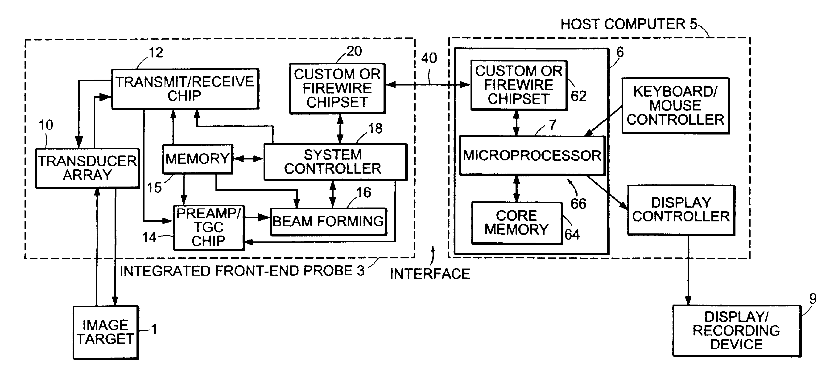
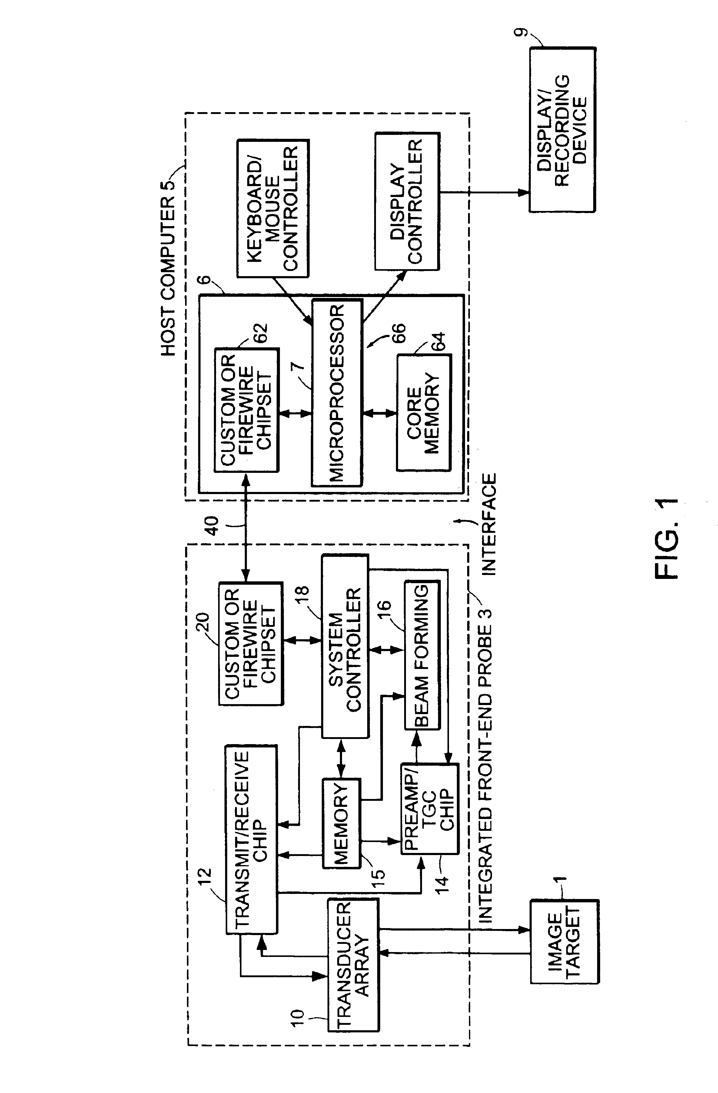
[0058]FIG. 1 is a schematic block diagram of an integrated probe system. Illustrated are a target object 1, a front-end probe 3, and a host computer 5, and a supplemental display / recording device 9. The front-end probe 3 integrates a transducer array 10 and control circuitry into a single hand-held housing. The control circuitry includes a transmit / receive module 12, a pre-amp / TGC module 14, a charge domain processor (CDP) beamforming module 16, and a system controller 18. Memory 15 stores program instructions and data. The CDP beamformer integrated circuit 16 includes a computational capacity that can be used to calculate the delay coefficients used in each channel. The probe 3 interfaces with the host computer 5 over a communications link 40, which can follow a standard high-speed communications protocol, such as the FireWire (IEEE P1394 Standards Serial Interface) or fast (e.g., 200 Mbits / second or faster) Universal Serial Bus (USB 2.0) protocol. The standard communication link t...
PUM
 Abstract
Description
Claims
Application Information
 - R&D
- Intellectual Property
- Life Sciences
- Materials
- Tech Scout
- Unparalleled Data Quality
- Higher Quality Content
- 60% Fewer Hallucinations
Browse by: Latest US Patents, China's latest patents, Technical Efficacy Thesaurus, Application Domain, Technology Topic, Popular Technical Reports.
© 2025 PatSnap. All rights reserved.Legal|Privacy policy|Modern Slavery Act Transparency Statement|Sitemap|About US| Contact US: help@patsnap.com


