
Configurable photonic device

a photonic device and configuration technology, applied in the field of manmade photonic crystals, can solve the problems of unintended imperfections, limitations in the fabrication process, and inability to readily find the periodicities of photonic crystals in nature, and achieve the effects of relaxed constraints, improved yields, and amenable to open loop control

Inactive Publication Date: 2005-11-01
THE KERR
View PDF18 Cites 27 Cited by
  • Summary
  • Abstract
  • Description
  • Claims
  • Application Information

AI Technical Summary

Benefits of technology

[0021]It has surprisingly been found that such effected changes in the physical geometry of region(s) of a photonic crystal can be used to control propagation and confinement of light in a discretionary fashion. The invention therefore offers the advantage of the hitherto unavailable combination of precise control of light propagation or confinement, or both, with the ability to route light propagation in a discretionary fashion based on geometrical configuration in a region.
[0028]Configuration also provides a mechanism for adaptively removing imperfections in a photonic crystal. For example, the imperfections characteristic of real structures may be compensated by using electric fields applied in a discretionary fashion to elements of the structure, throughout the structure. Also, this principle may be used to configure the photonic device by measuring the output signal(s) of the photonic device and applying input signal(s) to change the physical geometry of the device so as to provide for closed loop control. This approach, for example, can be used to improve yields in the fabrication of complex, integrated, light circuits. Such devices are also amenable to open loop control.
[0029]Configuration of the support or substrate allows a photonic crystal of arbitrary dielectric material to be selected. The advantage in this case is that the constraint of using a piezoelectric material is relaxed, and the opportunity to select materials with superior refractive index contrast is available. Using standard bonding technology, the photonic crystal can be mated to an array of actuators that change the geometry of the photonic crystal permitting defects to be introduced arbitrarily. MEMS technology is well suited for fabricating such arrays and readily offers the possibility of producing actuators capable of yielding displacements with sub-nanometer resolution.

Problems solved by technology

Photonic crystals having these corresponding periodicities are not readily available in nature.
For example, in a photonic crystal comprised of a periodic array of air-holes within a dielectric sheet, a possible defect would include leaving an array position with the dielectric material intact and not having an air-hole at that location.
It has been recognized that photonic crystals may also provide imperfect reflectivity (i.e., reflectivity less than unity) due to imperfections in the periodic structure, Such imperfections can act in a manner similar to defect states, but occur through inadvertence and often result from limitations in the fabrication process.
Although fabrication techniques have improved, unintended imperfections continue to occur and no practical means has been proposed to remove or correct them.
The main limitation of traditional photonic crystals is that control over the propagation or confinement of light is determined and fixed by its physical structure, as the defect state is permanently fixed in the photonic crystal, Although fixed defects in photonic crystals offer an ability to control light propagation or confinement, once such defects are introduced, the propagation or confinement of light in the crystal is determined.
Thus, discretionary switching of light, for example, or re-routing of optical signals, is not available with fixed defects in a photonic crystal.
However, known materials offer only low electro-optic coefficient values for applied electric fields below the breakdown limit, and thus yield only small changes in refractive index.
In this case, the refractive index contrast between the two media is significantly lowered, limiting the possibility of obtaining a full photonic bandgap.
), but the proposed method does not provide discretionary modification of selected elements of the photonic device.
None of the previously disclosed approaches for tuning photonic crystals has been successful in practical applications because they either provide only negligible changes in the ability of the structures to guide or confine light, or they significantly reduce the size of the photonic band gap, or they produce only non-local changes that are not useful for re-routing or confining light in a discretionary fashion.

Method used


Image

  • Configurable photonic device
  • Configurable photonic device
  • Configurable photonic device

Examples


Embodiment Construction

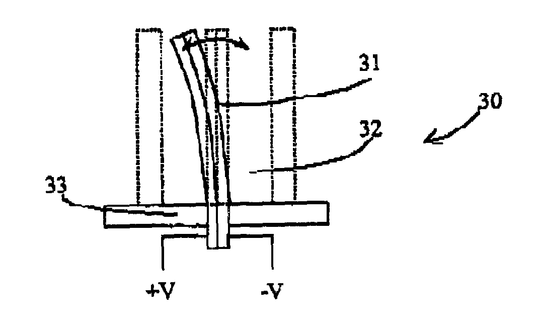
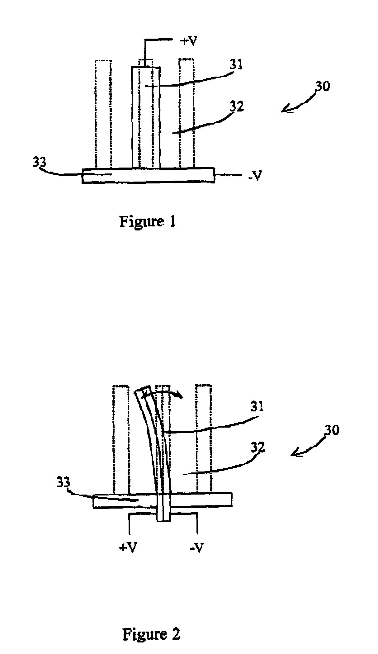
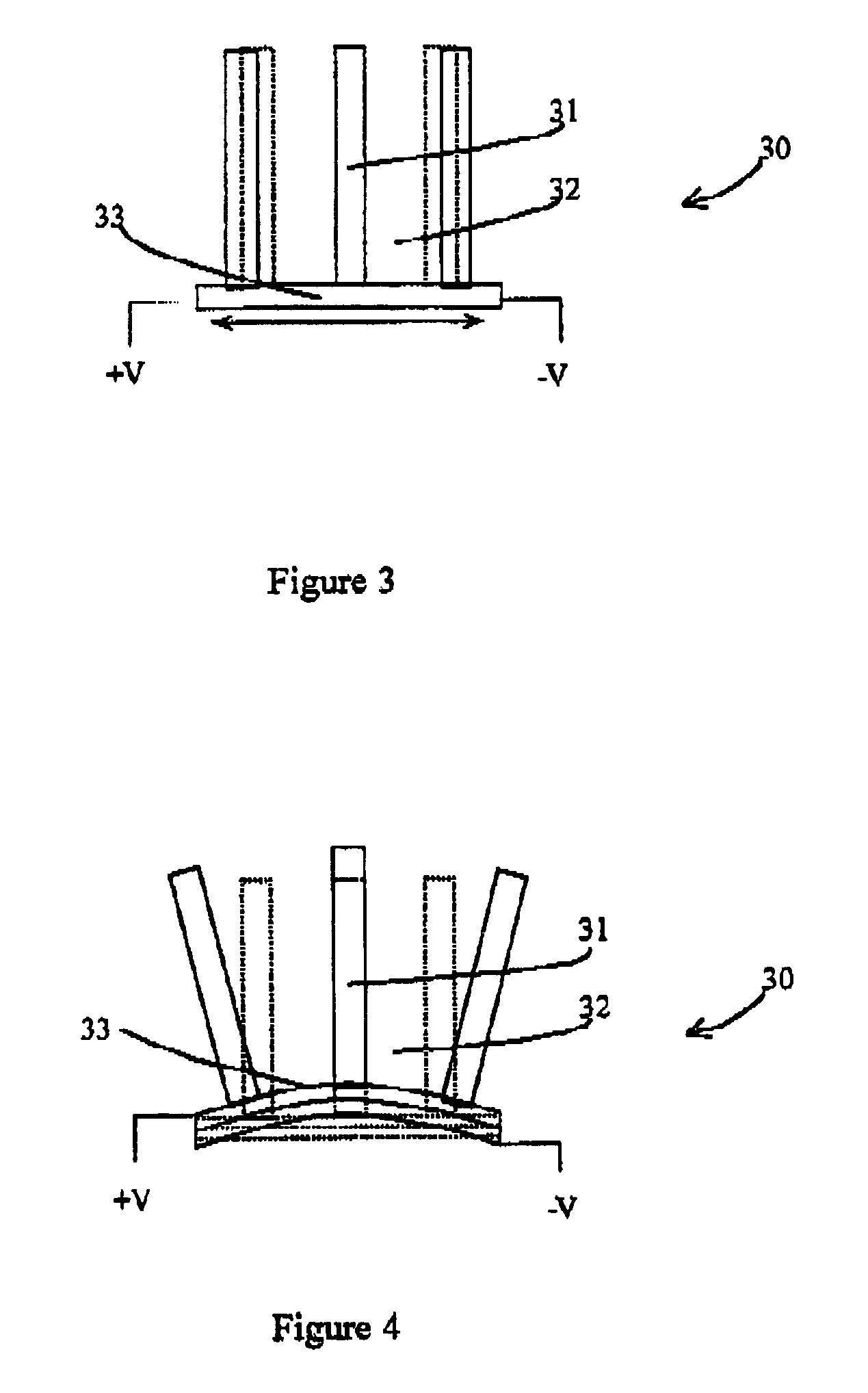
[0060]A first preferred embodiment of the invention, in which the physical geometry of a photonic crystal may be configured due its intrinsic (or material) properties, is shown schematically in FIG. 1. The photonic device comprises a photonic crystal 30 which includes pillars of a piezoelectric material 31 separated by air 32 on a support 33. A voltage applied across the piezoelectric pillar 31 will configure the pillar such that the dimensions (size or shape) of the pillar will be changed (from the dotted line to the solid line). The resulting change in periodicity will alter the optical properties of the photonic crystal.

[0061]An advantage of configuration of the photonic device element by directly changing the geometry of the photonic crystal itself is that it leads directly to changes in the optical properties of the photonic device. The benefit of configuration of the photonic device element using the support is that there is no restriction on the selected photonic crystal that...


PUM

PropertyMeasurementUnit
wavelengthsaaaaaaaaaa
reflectivityaaaaaaaaaa
refractive indicesaaaaaaaaaa

Abstract

A photonic crystal, and a photonic device having such a photonic crystal, configured by changing its physical geometry in at least one region to alter light propagation and / or confinement. The configuring means may include electrostrictive, piezoelectric or magnetostrictive components of the photonic crystal, or an actuation device affixed to the photonic crystal.

Description

[0001]This is an application claiming the benefit under 35 USC 119(e) of U.S. Provisional Application Ser. No. 60 / 222,481, filed Jul. 31, 2000. All of U.S. 60 / 222,481 is incorporated herein by this reference to it.FIELD OF THE INVENTION[0002]This invention relates generally to photonic devices, and more particularly to man-made photonic crystals suitable for use in controlling light propagation in photonic devices.BACKGROUND OF THE INVENTION[0003]Photonic crystals are periodic, dielectric, composite structures in which the interfaces between the dielectric media behave as scattering centres for light. Photonic crystals consist of at least two component materials (one of which may be air) having different refractive indices. The materials are arranged alternatingly in a periodic manner that is scaled so as to interfere with the propagation of light in a particular wavelength range. Light is scattered at the interfaces between the materials due to differences in the refractive index (...

Claims


Application Information

Patent Timeline
Patent Type & Authority Patents(United States)
IPC IPC(8): G02B6/35G02B6/43G02B6/122G02F1/01
CPCB82Y20/00G02B6/1225G02B6/351G02B6/3534G02F1/0128G02B6/3546G02B6/3556G02B6/357G02B6/3572G02B6/3578G02B6/43G02F2202/32
Inventor MATSUURA, NAOMIRUDA, HARRY E.YACOBI, BEN G.
Owner THE KERR
Learn More