
Organic light-emitting devices including specific barrier layers

a technology of organic light-emitting devices and specific barrier layers, which is applied in the direction of discharge tube luminescnet screens, discharge tube/lamp details, electric discharge lamps, etc., and can solve the problems of non-emitting black spots, prone to reactive ambient species reaction, and consequent degradation of device performan

Inactive Publication Date: 2005-11-01
CAMBRIDGE DISPLAY TECH LTD
View PDF28 Cites 12 Cited by
  • Summary
  • Abstract
  • Description
  • Claims
  • Application Information

AI Technical Summary

Benefits of technology

[0004]It is therefore an aim of the present invention to provide an organic light-emitting device which is less prone to the formation of non-emitting black spots and therefore displays improved resistance to performance degradation.
[0005]It is another aim of the present invention to provide a method of producing a protective cap for an electrode of an organic light-emissive device which minimizes damage to the underlying organic layers.
[0008]The inert barrier layer serves to minimize the entry of reactive species into the device, and the gettering layer serves to absorb any traces of reactive species which manage to somehow permeate through the inert barrier layer.
[0013]In one embodiment of the present invention, the organic light-emitting device further comprises a second layer of dielectric material on the first layer of dielectric material, the thickness of the dielectric layers being selected so as to reduce mechanical stress on the electrode.
[0019]As with the first and second aspects of the present invention, the advantages of the third aspect of the present invention are pronounced when the subject electrode has been deposited by a vacuum evaporation technique.

Problems solved by technology

However, it is an intrinsic property of such low work function elements that they are very prone to reactions with reactive ambient species such as oxygen or moisture.
Such reactions detrimentally affect the electron-injecting properties of the cathode causing the formation of non-emitting black spots with a consequent degradation in device performance.

Method used


Image

  • Organic light-emitting devices including specific barrier layers
  • Organic light-emitting devices including specific barrier layers
  • Organic light-emitting devices including specific barrier layers

Examples


first embodiment

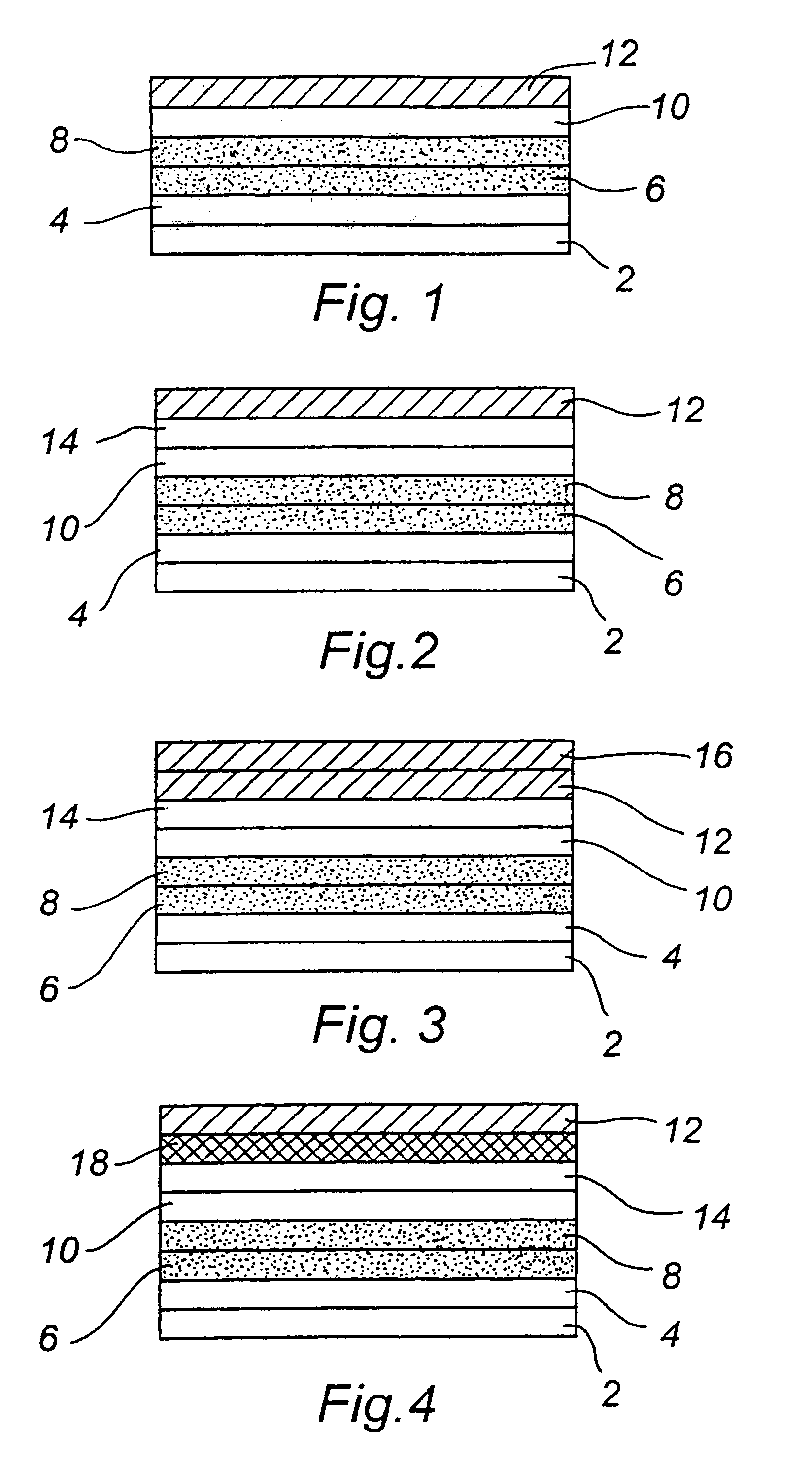
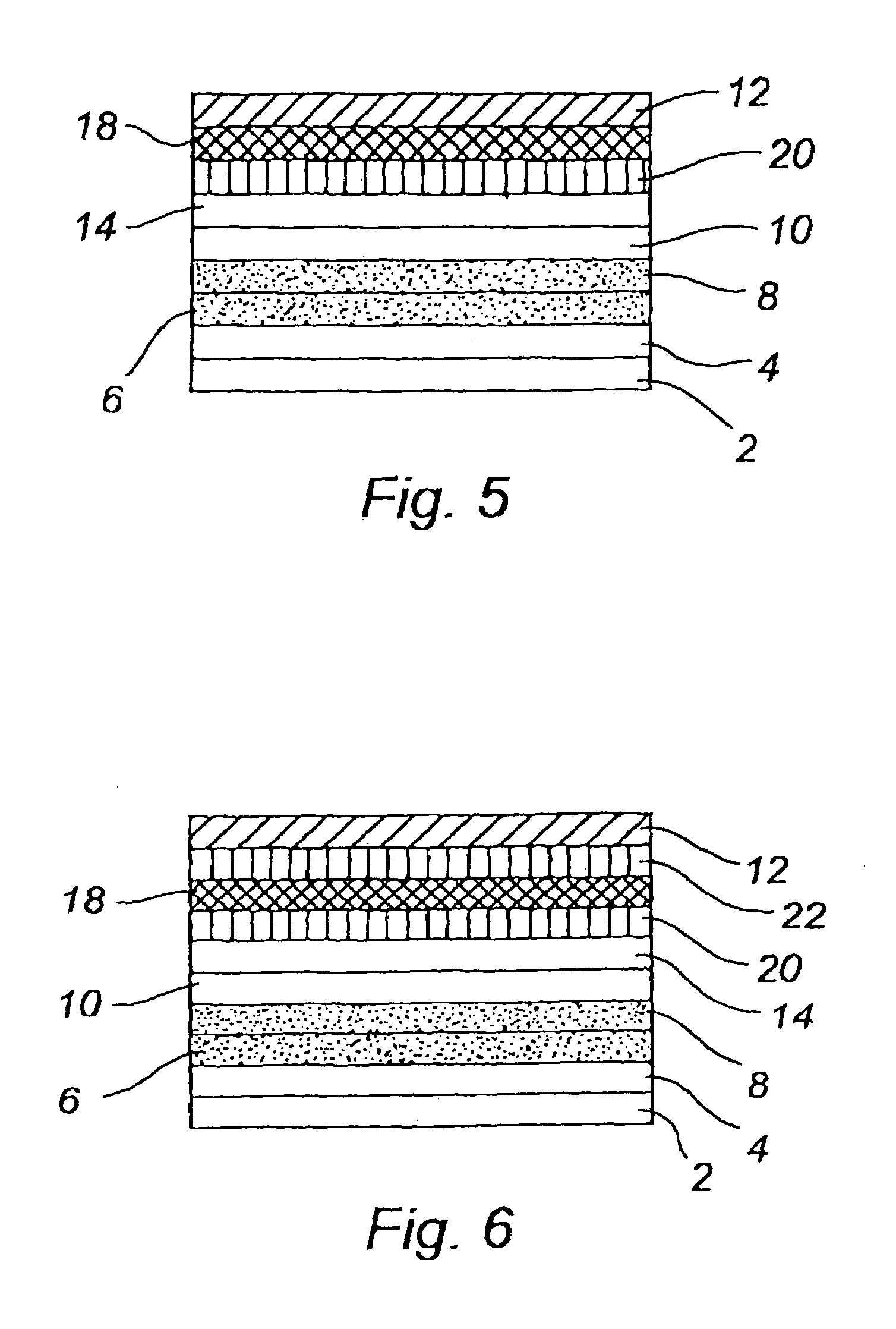
[0028]An organic light-emitting device according to the present invention is shown in FIG. 1. The device comprises a first electrode layer 4, in this case an anode layer comprised of indium tin oxide (ITO) formed on a substrate 2. The substrate may, for example, be one made of glass or a flexible plastic substrate or may be a glass-plastic laminate. A first thin film 6 of a light-emissive organic material (in this case, poly(phenylenevinylene) (PPV)) is formed on the ITO layer 4. This organic PPV layer can be formed by spin-coating a precursor to PPV in a suitable solvent onto the ITO layer and then heating the spin-coated layer to convert the precursor to the polymer PPV. A second thin film 8 of an organic material (such as MEH-PPV) is formed on the first thin film of light-emissive organic material 6. This second thin film 8 can, for example, be formed in the same general manner as the first thin film 6 of light-emissive organic material. The second thin film of organic material m...

second embodiment

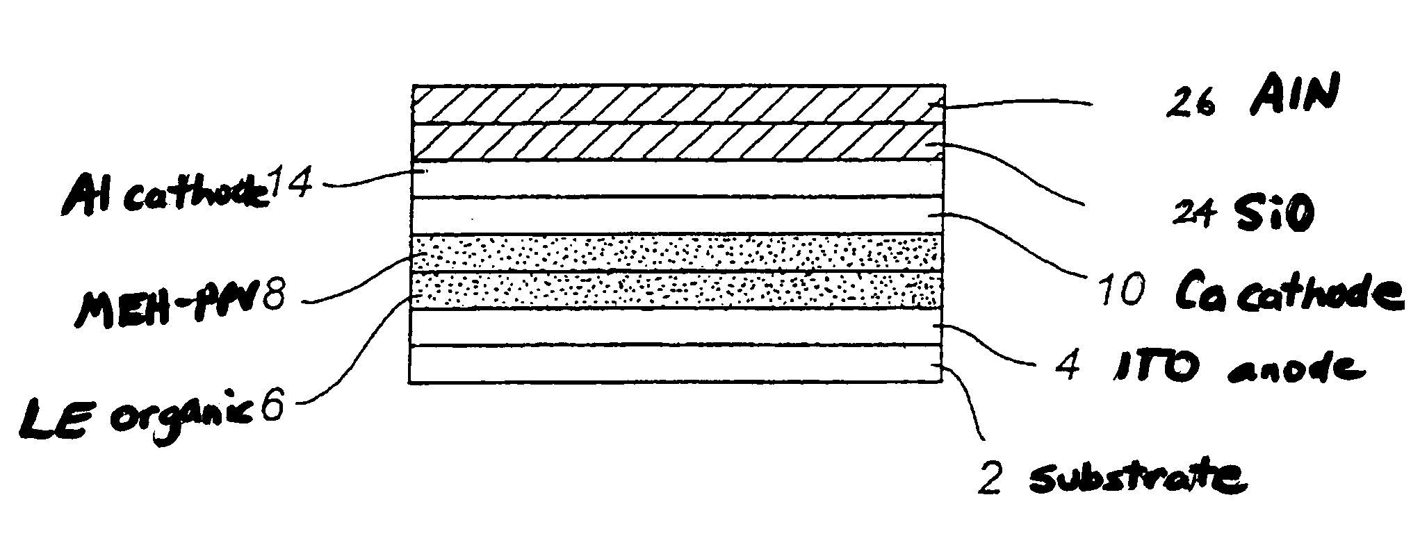
[0033]An organic light-emitting device according to the present invention is shown in FIG. 2. It is identical to the device shown in FIG. 1 except that an additional layer 14 of aluminium having a thickness of 5 microns is provided between the thin calcium layer 10 and the thick layer of aluminium nitride 12 as a second cathode layer. In this case, this intermediate layer of aluminium is formed by vacuum evaporation, but it could alternatively be formed by a sputtering technique for example.

third embodiment

[0034]An organic light-emitting device according to the present invention is shown in FIG. 3. It is similar to the device shown in FIG. 2 except that a thick layer 16 of aluminium oxide having a thickness of about 10 microns is provided on the thick layer of aluminium nitride 12. This top layer of aluminium oxide is preferably formed by a sputtering technique in order to provide a pinhole-free layer.


PUM


Abstract

An organic light-emitting device comprising a layer of light-emissive organic material interposed between a first electrode and a second electrode, at least one of the first and second electrodes comprising one or more electrode layers on the layer of light-emissive organic material for injecting charge carriers into the light-emissive organic material, wherein the organic light-emitting device further comprises a layer of dielectric material on the surface of the outermost electrode layer remote from the layer of light-emissive organic material.

Description

[0001]This invention relates to organic light-emitting devices (OLEDs).FIELD OF THE INVENTION[0002]Organic light-emitting devices such as described in U.S. Pat. No. 5,247,190 or in U.S. Pat. No. 4,539,507, the contents of which are incorporated herein by reference, have great potential for use in various display applications. According to one method, an OLED is fabricated by coating a glass or plastic substrate with a transparent first electrode (anode) such as indium tin oxide (ITO). At least one layer of a thin film of an electroluminescent organic material is then deposited prior to a final layer which is a film of a second electrode (cathode) which is typically a metal or alloy.BACKGROUND OF THE INVENTION[0003]From the point of view of electron-injecting properties, a layer of a metal having a low work function such as calcium or an alloy containing a metal having a low work function are the preferred materials for the cathode. However, it is an intrinsic property of such low wo...

Claims


Application Information

Patent Timeline
IPC IPC(8): H01L51/52H01L51/50H05B33/04H05B33/26
CPCH01L51/5237H10K50/846H10K50/844
Inventor HEEKS, STEPHEN KARLBURROUGHES, JEREMY HENLEYCARTER, JULIAN CHARLESDEVINE, PETER
Owner CAMBRIDGE DISPLAY TECH LTD
Learn More