Phase comparator circuit
a comparator circuit and phase technology, applied in the direction of oscillation comparator circuits, automatic control of pulses, instruments, etc., can solve the problems of large fluctuation in the phase of the circuit, inability to discriminate correctly, and difficulty in reducing the size of the optical transceiver modul
- Summary
- Abstract
- Description
- Claims
- Application Information
AI Technical Summary
Benefits of technology
Problems solved by technology
Method used
Image
Examples
first embodiment
(b) First Embodiment
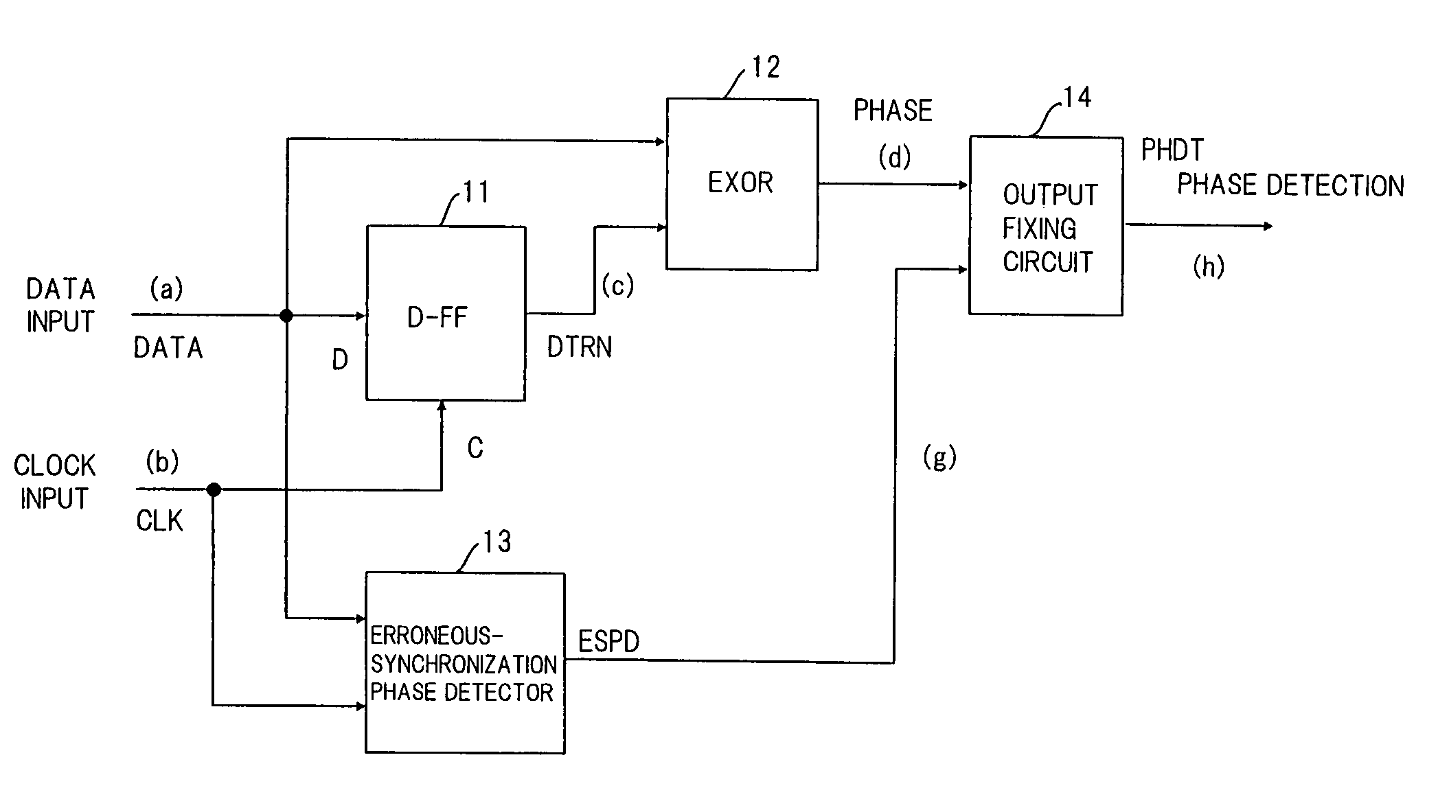
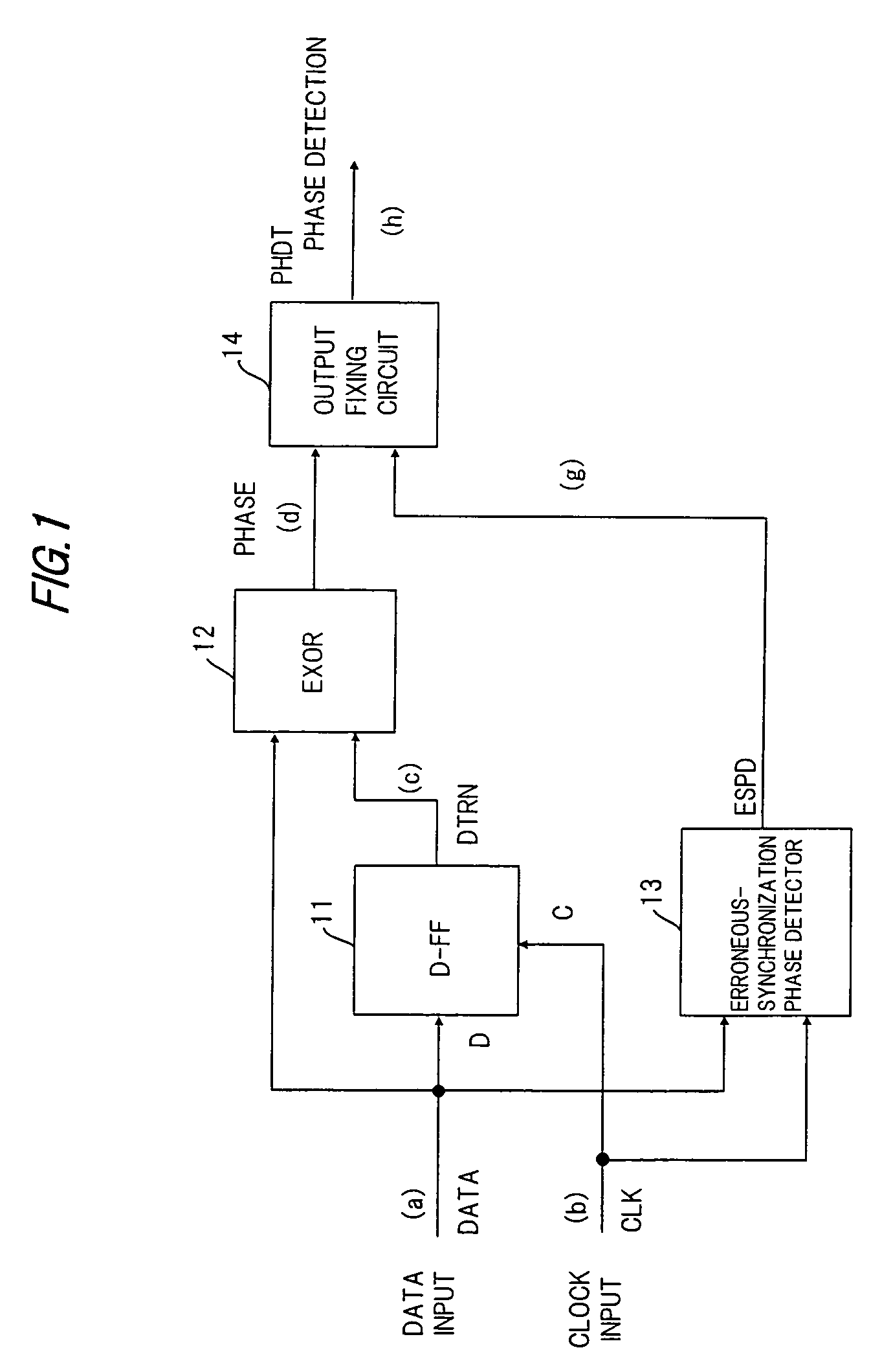
[0088]FIG. 13 is a block diagram showing a phase comparator circuit which is a first embodiment of the third aspect of the present invention. Components in FIG. 13 identical with those shown in FIG. 1 are designated by like reference characters. The circuit includes the first D-type flip-flop (D-FF1) 11, the EX-OR circuit 12 for outputting a signal that conforms to the phase difference between the data signal DATA and the clock signal CLK, an erroneous-synchronization phase detector 31 for detecting whether the phase difference between the data signal DATA and the clock signal CLK resides within a range of phases (0 to π / 2, 3π / 2 to 2π) for which there is a possibility of erroneous synchronization, a latch circuit 32 for outputting the phase detection signal PHDT, and a latch timing circuit 33 for deciding latch timing.
[0089]If the duty of the data signal is (100−d)(%) to (100+d)(%), then the range of phases for which there is a possibility of erroneous synchroniz...
second embodiment
(c) Second Embodiment
[0100]FIG. 19 is a block diagram showing a phase comparator circuit which is a second embodiment of the third aspect of the present invention. Components in FIG. 19 identical with those shown in FIG. 13 are designated by like reference characters. This embodiment differs from the first embodiment in that whereas the falling edge of the clock signal CLK is the latch timing in the first embodiment, the latch timing in the second embodiment is that following elapse of a period of time, which corresponds to the phase n, from the rising edge of the data signal DATA. Operation of the second embodiment is identical with that of the first embodiment in other respects.
[0101]The phase comparator circuit according to this embodiment includes the first D-type flip-flop (D-FF1) 11, the EX-OR circuit 12 for outputting a signal that conforms to the phase difference between the data signal DATA and the clock signal CLK, the erroneous-synchronization phase detector 31 for detect...
third embodiment
(d) Third Embodiment
[0107]FIG. 21 is a block diagram showing a phase comparator circuit which is a third embodiment of the third aspect of the present invention. Components in FIG. 21 identical with those shown in FIG. 13 are designated by like reference characters. This embodiment differs from the first embodiment in the construction of the erroneous-synchronization phase detector 31; the two embodiments are identical in construction in all other respects.
[0108]The erroneous-synchronization phase detector 31 includes a first delay circuit 41 for delaying the clock signal CLK by a length of time corresponding to the phase π, a second delay circuit 42 for delaying the data signal DATA by a length of time corresponding to phase π / 2, an inverter 43 for inverting the polarity of the polarity of the delayed clock signal, a NAND gate 44 for computing the NAND between the clock signal CLK (b) and the delayed inverted clock signal output by the inverter 43, and a D-type flip-flop (D-FF2) fo...
PUM
 Abstract
Description
Claims
Application Information
 - R&D
- Intellectual Property
- Life Sciences
- Materials
- Tech Scout
- Unparalleled Data Quality
- Higher Quality Content
- 60% Fewer Hallucinations
Browse by: Latest US Patents, China's latest patents, Technical Efficacy Thesaurus, Application Domain, Technology Topic, Popular Technical Reports.
© 2025 PatSnap. All rights reserved.Legal|Privacy policy|Modern Slavery Act Transparency Statement|Sitemap|About US| Contact US: help@patsnap.com


