Method and apparatus for inspecting printed circuit boards

Inactive Publication Date: 2005-08-30
ORMON CORP
View PDF24 Cites 31 Cited by
  • Summary
  • Abstract
  • Description
  • Claims
  • Application Information

AI Technical Summary

Benefits of technology

[0020]In any of the above-mentioned methods, a circuit board is observed in a non-contact state to the circuit board by a method except for the image-pickup method, and the determining process is carried out by detecting a physical quantity representing whether or not any defect exists. Here, even when the defective portion is extremely small or the degree of the defect is small, by obtaining the detected physical quantity (a state of change in the electric field or magnetic field, or a level of a reflected wave of the ultrasonic wave) as a voltage that is sufficiently great, it is possible to detect this defect with high precision, and even when the inspection object is a circuit board with high density, it is possible to carry out the inspection with high precision without causing any damage to the circuit of the circuit board. Moreover, with respect to a circuit including a part formed by a face-down assembling process, it is possible to carry out inspection processes in a non-contact state.
[0021]Moreover, in any of the above-mentioned methods, even when an area including circuit patterns or parts that constitute a redundant circuit is an object of inspection in the above-mentioned printed circuit board, it is possible to detect any defect occurring in any one of the branched circuits, and consequently to greatly improve the inspection precision.
[0022]Here, in the first method of the above-mentioned three methods, any defect is detected based upon a change in the electric field or magnetic field in response to an electric potential or an electric current occurring in the circuit upon application of a current; therefore, if, even when a defect such as short-circuiting occurs, the defect causes no abnormal value in the electrical potential and current in the defective portion in association with the other circuits, it becomes impossible to detect the defect. In contrast, in the second and third method, the determining process is carried out by using a physical quantity representing a state of a wiring pattern and a part without applying any current to the circuit board, it becomes possible to detect a defective portion that the first method would fail to detect.
[0025]In the case when the above-mentioned detection unit detects an electric field, the detection unit is provided with a detection electrode which allows an electrostatic capacity to be exerted between the circuit board and the detection unit so as to detect this electrostatic capacity, and a shielding electrode that is used for shielding influences of an electric field from a direction other than the circuit board from being exerted on the detection electrode. Moreover, in the case when the determining process is carried out by using a magnetic field, the detection unit is preferably provided with devices such as a magnetic resistor element like an magnetic induction (MI) element and an oscillator for allowing a high frequency current to flow this element, and a means like a bias magnet for generating a bias magnetic field so as to improve the sensitivity of the element.
[0026]Here, in the case when either of the electric field and magnetic field is detected, the detection unit is desirably arranged so that an electric field or a magnetic field is detected at a plurality of positions so as to eliminate noise signals and to output a differential signal (that is, a change in the electric field or magnetic field in a predetermined pitch) of the detection signals obtained from the respective positions.

Problems solved by technology

Along with the recent developments in printed circuit boards with high-density, extremely fine parts and wiring patterns, it has become difficult to correctly put test probes onto portions to be inspected in the case of inspections using an in-circuit tester.
Moreover, when test probes are put onto a printed circuit board having a high density, the circuit board might be damaged due to a disconnection in the wiring pattern.
In the case of a circuit board used for an apparatus requiring a high degree of safety, a redundant circuit such as a duplexed circuit is formed therein, and with respect to such a redundant circuit, test probes are put at a position before the branch of the respective circuits and at a position after the branch; therefore, even when there is any defect in one portion of the pattern, if the other pattern is normal, the detected electrical potential by the test probes shows the same value as the normal value, thereby failing to properly detect a defect.
Moreover, with respect to parts that have been packaged by using a face-down packaging method, since connecting portions cannot be recognized from the face side of the circuit board, it is impossible to carry out the detecting process by using a visual recognition device.

Method used


Image

  • Method and apparatus for inspecting printed circuit boards
  • Method and apparatus for inspecting printed circuit boards
  • Method and apparatus for inspecting printed circuit boards

Examples


Embodiment Construction

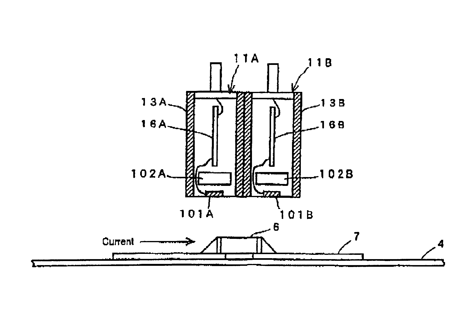
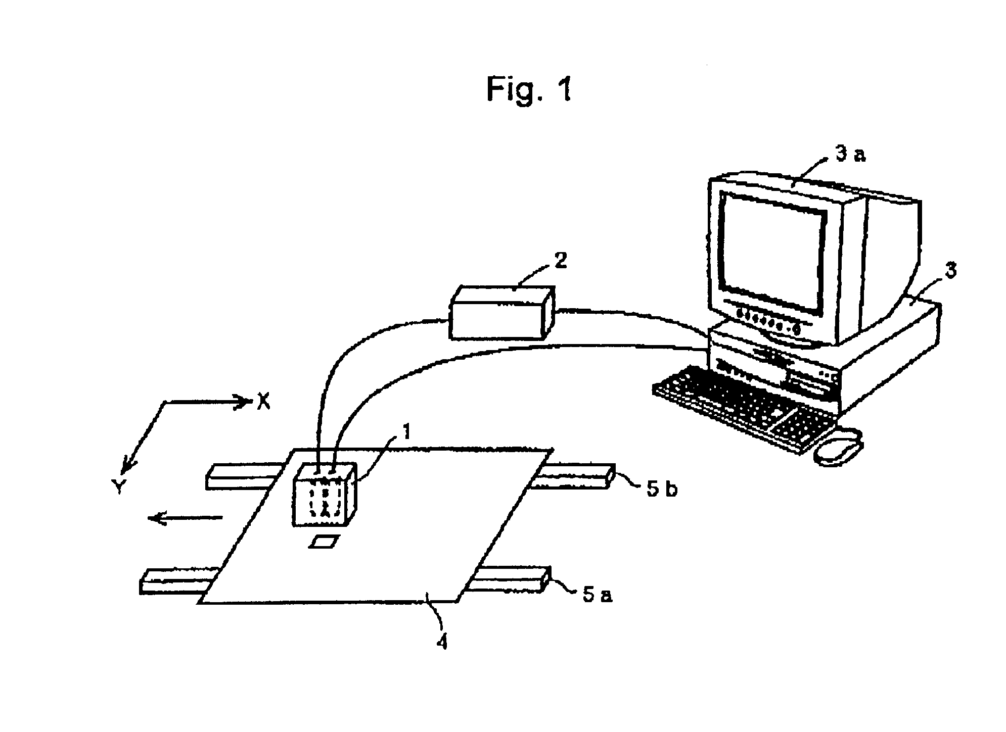
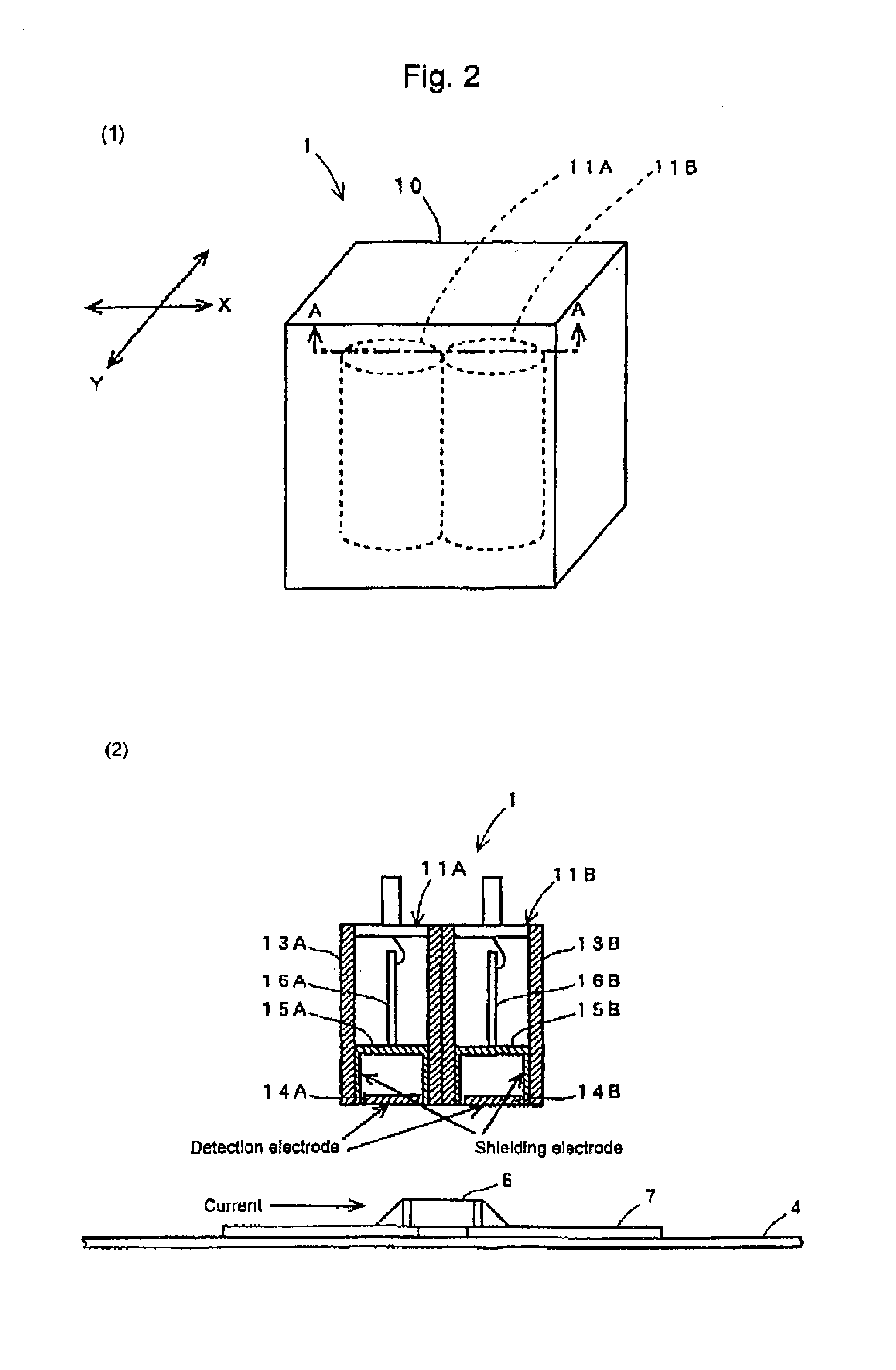
[0058]FIG. 1 shows a schematic structure of an inspection apparatus in accordance with one preferred embodiment of the present invention. This inspection apparatus is used for detecting defects such as a disconnection and short-circuiting of a wiring pattern, a breakdown and a defective mounting of a part on a printed circuit board 4 (hereinafter, simply referred to as “circuit board 4”) in a non-contact state to the circuit board 4, and is constituted by a detection unit 1 placed at a position above the circuit board 4, as well as a position adjusting device 2, a control device 3, etc.

[0059]A circuit board 4 to be inspected is placed on transporting-use rails 5a, 5b, and is transported by a driving mechanism, not shown, and positioned to a predetermined inspection position. The above-mentioned position adjusting device 2 controls a positioning mechanism (not shown) in the detection unit 1 so that the position of the detection unit 1 is adjusted in the respective X and Y axis direct...


PUM


Abstract

A detection unit for detecting an electric field or a magnetic field is placed above a circuit to be detected. A control device allows the detection unit 4 to carry out detection processes while moving the detection unit in a predetermined direction with an electric current being applied to the circuit board so that an electric field distribution or a magnetic field distribution on the circuit board is detected. Moreover, the control device compares the results of the diction with reference data that has been preliminarily registered, and if there is any portion between the two pieces of data that is not coincident with each other, it is determined that the corresponding circuit board is a defective circuit board. Thus, it is possible to detect any defective portion on the printed circuit with high precision in a non-contact state to the circuit board.

Description

BACKGROUND OF THE INVENTION[0001]1. Field of the Invention[0002]The present invention relates to a technique for inspecting a circuit board on which various parts are packaged (hereinafter, referred to as “printed circuit board”) for any defect such as a disconnection and a short-circuiting of a wire pattern, a defective part, a positional deviation, a raised state of a part, insufficient and exceeding soldering processes and a breakdown of a part.[0003]2. Description of the Background Art[0004]With respect to inspections of this type, conventionally, an inspection using an in-circuit tester has been carried out. In this inspection, as shown in FIG. 20, after an electric current has been applied to a printed circuit board 4, two points are selected from a wiring pattern 7 and terminals 6a, 6b of a part 6 to be inspected, and test probes 31, 32 are applied to these points so that factors, such as an electric current, a voltage, an impedance or a frequency, are measured between the tw...

Claims


Application Information

Patent Timeline
IPC IPC(8): G01R31/315G01R31/28G01R31/02H05K3/34H05K13/08
CPCG01R31/315
Inventor KAWAIKE, NOBORUUEDA, KENJIMATSUI, KENJI
Owner ORMON CORP
Why Eureka
Try Eureka