Ultimate analyzer, scanning transmission electron microscope and ultimate analysis method

a technology of transmission electron microscope and analyzer, which is applied in the direction of material analysis using wave/particle radiation, instruments, nuclear engineering, etc., can solve the problems of difficult to obtain element distribution in real time, large volume of measured data, and long time to obtain two-dimensional images, etc., to achieve high contrast and high accuracy

Inactive Publication Date: 2005-08-23
HITACHI LTD
View PDF13 Cites 8 Cited by
  • Summary
  • Abstract
  • Description
  • Claims
  • Application Information

AI Technical Summary

Benefits of technology

[0021]An object of the present invention is to provide an ultimate analyzer which can display an element distribution image of an object to be analyzed with high contrast to determine the positions of the element distribution with high accuracy, and a scanning transmission electron microscope and a method of analyzing elements using the ultimate analyzer.

Problems solved by technology

Since it is necessary to perform the repetitive operation described above for all the measuring points, it takes a long time to obtain a two-dimensional image, and accordingly it is difficult to obtain an element distribution in real time.
In this method, the volume of measured data becomes very large, and further, the element distribution image can not be obtained in real time.
In addition to the above, in the case where the element distribution image can not be obtained in real time, there are following problems:
(B) The conventional analyzer is not suitable for the work such as the inspection to measure many samples because it requires the measurement of the electron energy loss spectra and the many complicated and complex operations for each measured point, and also it requires a long time for the measurement and the analysis.
Further, in an analyzer which detects an element to be analyzed by dividing an intensity of a first electron beam in an energy range containing a core-loss peak among the electron energy loss spectra of the element to be measured by an intensity of a second electron beam in an energy range higher than the core-loss peak, which is called as a jump-ratio method, there is the following problem depending on the sample to be analyzed.
In that case, since the contrast difference between a metal portion and an oxide or nitride portion becomes small, it becomes difficult to judge correctly existence of oxide or nitride.
As described above, the analyzer combining the electron energy loss spectrometer and the STEM is difficult to observe an element distribution image having high contrast in real time and to determine the distribution of the element with high accuracy.
However, this patent discloses a means for improving image quality of a STEM image, but not a means for analyzing elements of the sample.
However, this method is still not enough to respond to the demand for more contrasted screen-displaying of gate electrodes and oxidized films thereon.

Method used


Image

  • Ultimate analyzer, scanning transmission electron microscope and ultimate analysis method
  • Ultimate analyzer, scanning transmission electron microscope and ultimate analysis method
  • Ultimate analyzer, scanning transmission electron microscope and ultimate analysis method

Examples


Embodiment Construction

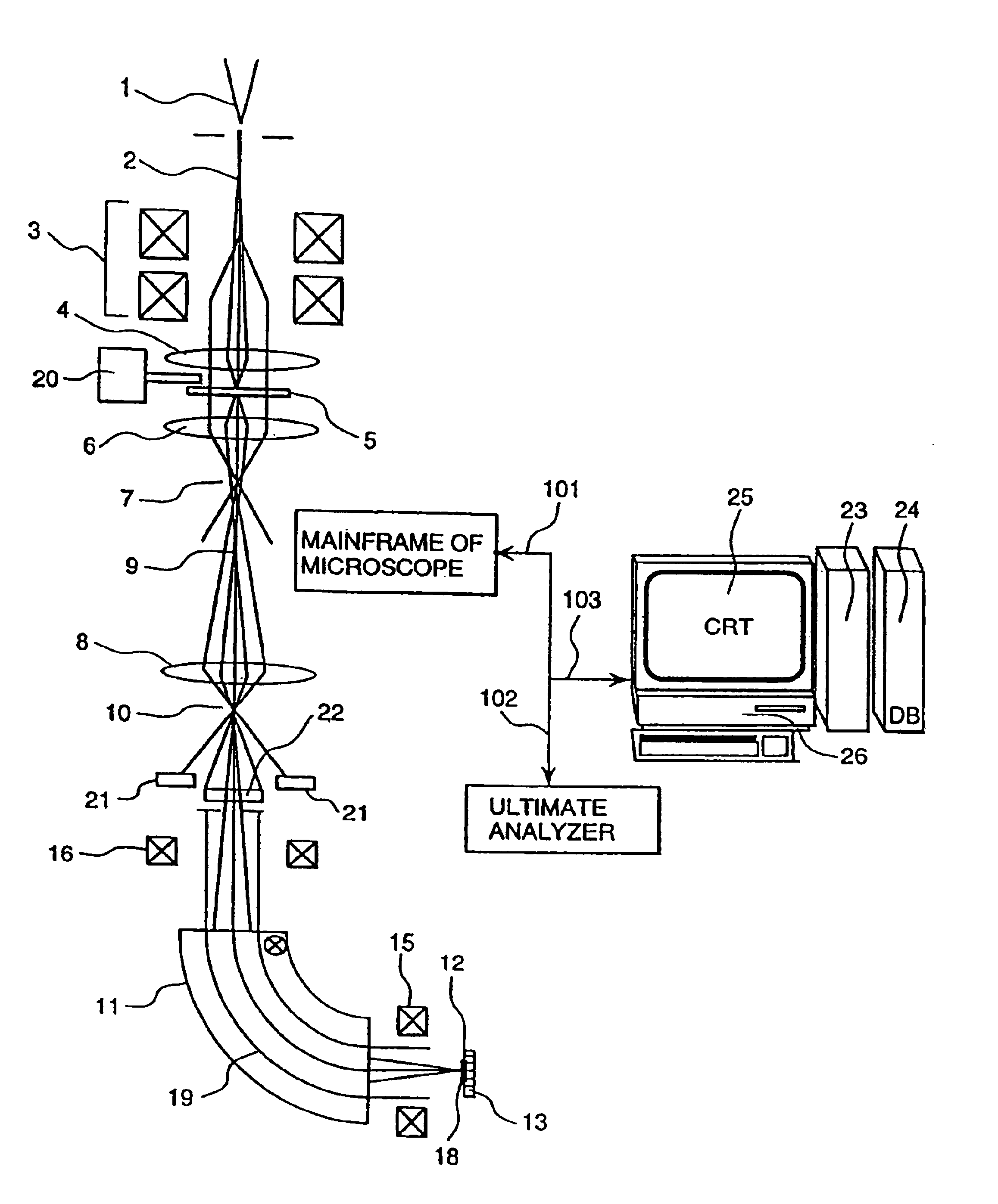
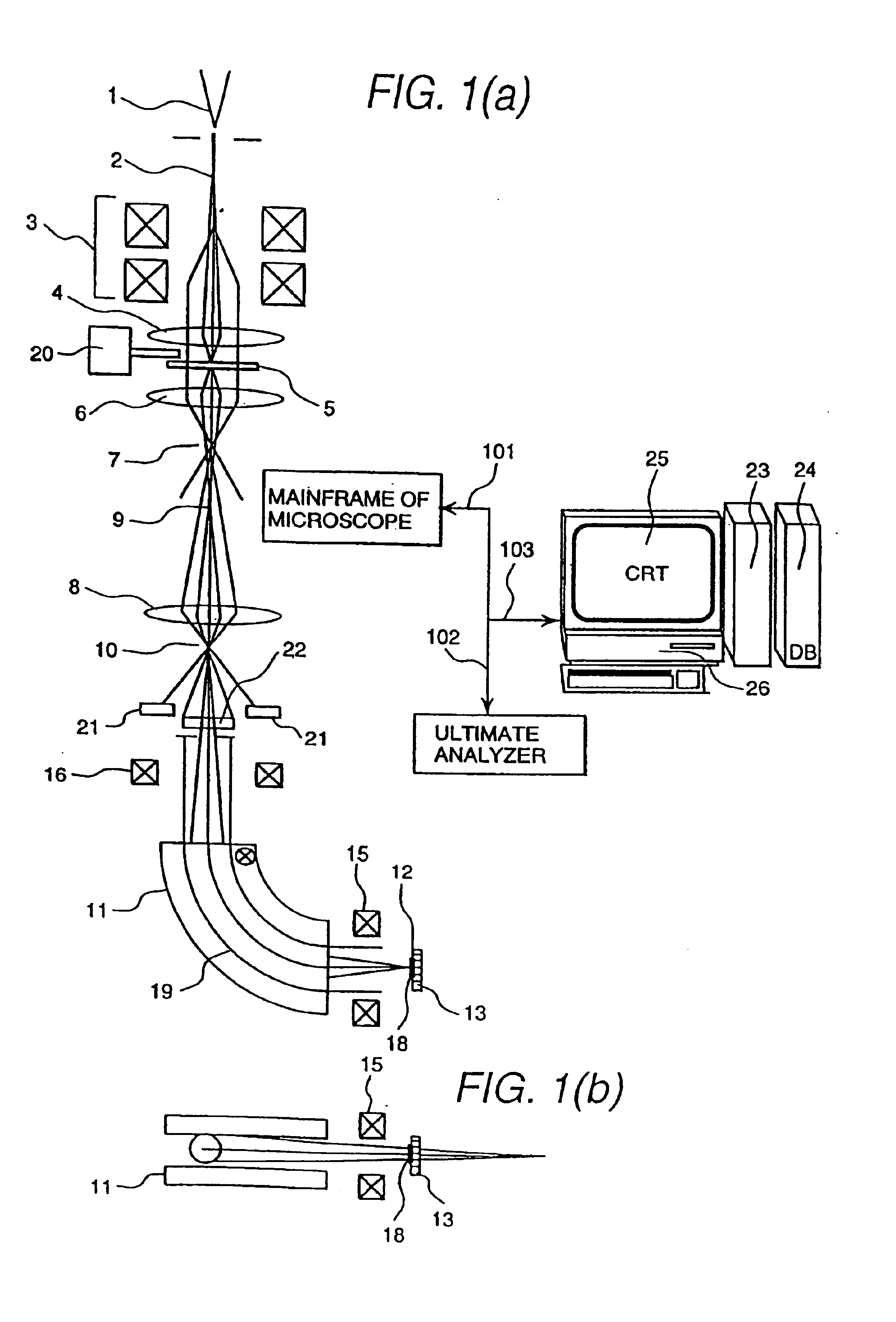
[0042]FIG. 1 is a schematic block diagram showing the main portion of a scanning transmission electron microscope (hereinafter, referred to as an electron microscope) having an embodiment of an ultimate analyzer in accordance with the present invention. FIG. 1(a) is a front view, and FIG. 1(b) is a view (a top view) seeing FIG. 1(a) from an electron beam source 1. In this figure, the portion from the electron beam source 1 to a phase contrast detector 22 is indicated as the mainframe of the electron microscope. The mainframe of the electron microscope includes a component for controlling scanning of an electron beam, not shown, used for exerting the function as the electron microscope.

[0043]Further, the portion from a scattered electron beam detector 21 to an electron beam detector 13 is indicated by an ultimate analyzer. A signal to a control unit 26 and a signal from the control unit 26 are transmitted through a signal line 103. An input unit such as a keyboard and so on and a pro...


PUM


Abstract

The present invention provides an ultimate analyzer which displays an element distribution image of an object with high contrast and high accuracy. A scanning transmission electron microscope and a method of analyzing elements using the ultimate analyzer is also provided. The ultimate analyzer comprises a scattered electron beam detector for detecting an electron beam scattered by an object; an electron spectrometer for energy dispersing an electron beam transmitted through the object; an electron beam detector for detecting said dispersed electron beam; and a control unit for analyzing elements based on an output signal of the electron beam detected by the electron beam detector and an output signal of the electron beam detected by the scattered electron beam detector.

Description

[0001]This application is a continuation of U.S. patent application Ser. No. 10 / 196,577, filed Jul. 17, 2002 (Notice of Allowance dated Dec. 11, 2003), which in turn is a continuation-in-part of U.S. patent application Ser. No. 10 / 069,793, filed Apr. 3, 2002 (now abandoned), which in turn was filed based on Application No. PCT / JP01 / 09618, filed Nov. 2, 2001, the entire disclosure of which is incorporated herein by reference.BACKGROUND OF THE INVENTION[0002]The present invention relates to a novel ultimate analyzer for analyzing elements of an object to be analyzed based on an output signal of a scattered electron beam and a plurality of output signals of an electron beam energy dispersed after passing through an object to be analyzed, and a scanning transmission electron microscope having the ultimate analyzer and an ultimate analysis method using the scanning transmission electron microscope.[0003]With progressing of miniaturizing and downsizing of semiconductor devices and magneti...

Claims


Application Information

Patent Timeline
IPC IPC(8): G01N23/04G01N23/02G01N23/20H01J37/256
CPCG01N23/04G01N23/20H01J37/05H01J37/244H01J37/256H01J37/265H01J37/28H01J2237/057H01J2237/24475H01J2237/24485H01J2237/24495H01J2237/2522H01J2237/2802H01J2237/2804H01J2237/2809
Inventor KAJI, KAZUTOSHIAOYAMA, TAKASHITAYA, SHUNROKUTANAKA, HIROYUKIISAKOZAWA, SHIGETO
Owner HITACHI LTD
Why Eureka
Try Eureka