Method of TiSiN deposition using a chemical vapor deposition (CVD) process

a technology of chemical vapor deposition and tisin, which is applied in the direction of vacuum evaporation coating, plasma technique, coating, etc., can solve the problems of unsatisfactory metal diffusion, adversely affecting the adhesion/barrier properties, and the resistivity of the titanium silicide nitride (tisin) layer

Inactive Publication Date: 2005-08-23
APPLIED MATERIALS INC
View PDF20 Cites 12 Cited by
  • Summary
  • Abstract
  • Description
  • Claims
  • Application Information

AI Technical Summary

Problems solved by technology

Such metal diffusion is undesirable because it would change the characteristics of the transistor, or render it inoperative.
However, when a TiCl4-based chemistry is used to form the titanium silicide nitride (TiSiN) layer, reliability problems are encountered.
In particular, by-products

Method used


Image

  • Method of TiSiN deposition using a chemical vapor deposition (CVD) process
  • Method of TiSiN deposition using a chemical vapor deposition (CVD) process
  • Method of TiSiN deposition using a chemical vapor deposition (CVD) process

Examples


Embodiment Construction

Wafer Processing System

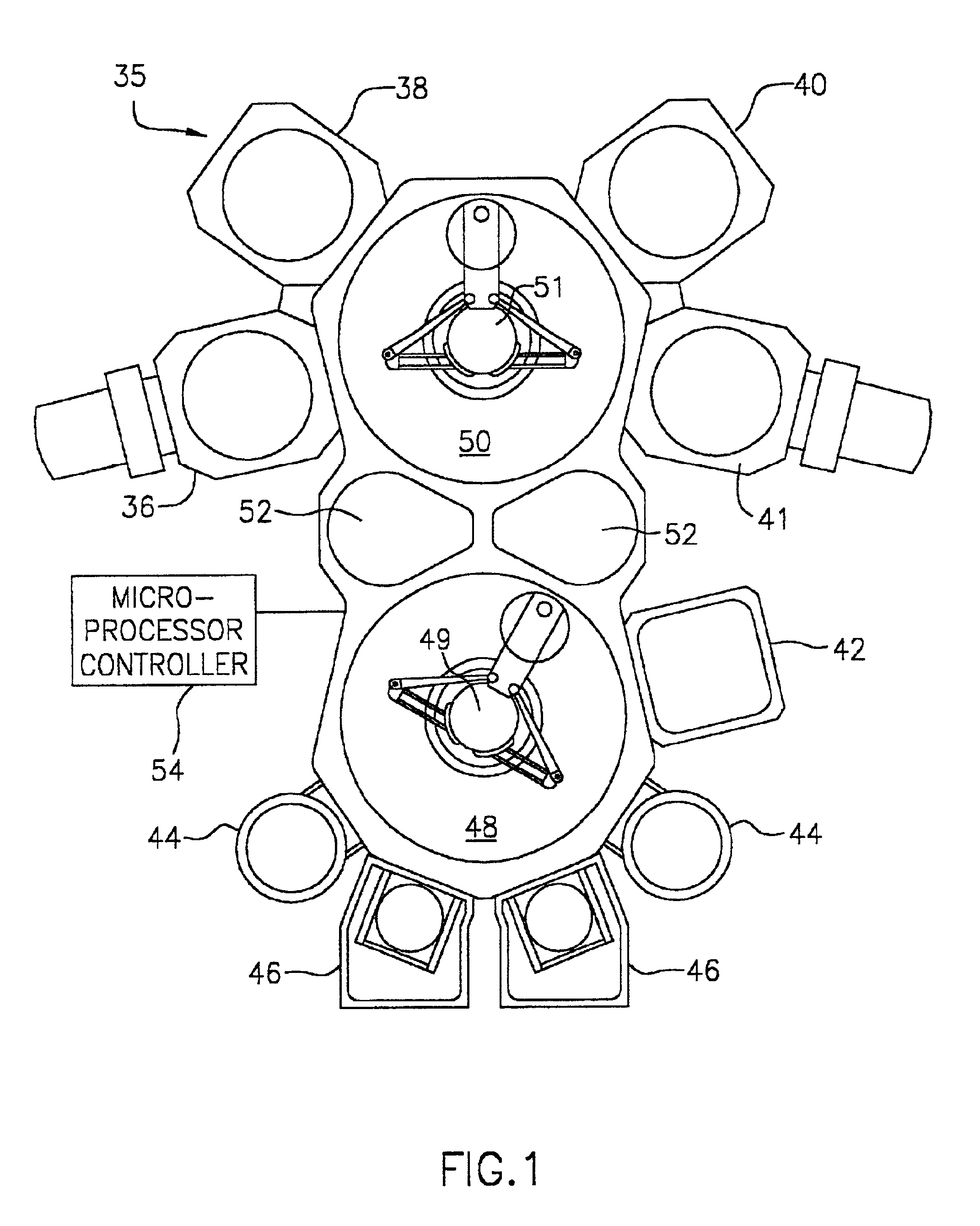
[0022]FIG. 1 is a schematic representation of a wafer processing system 35 that can be used to perform integrated circuit fabrication in accordance with embodiments described herein. The wafer processing system 35 typically comprises process chambers 36, 38, 40, 41, degas chambers 44, load-lock chambers 46, transfer chambers 48, 50, pass-through chambers 52, a microprocessor controller 54, along with other hardware components such as power supplies (not shown) and vacuum pumps (not shown). An example of such a wafer processing system 35 is an ENDURA® System, commercially available from Applied Materials, Inc., Santa Clara, Calif.

[0023]Details of the wafer processing system 35 are described in commonly assigned U.S. Pat. No. 5,186,718, entitled “STAGED-VACUUM SUBSTRATE PROCESSING SYSTEM AND METHOD”, issued Feb. 16, 1993, and is hereby incorporated by reference. The salient features of the wafer processing system 35 are briefly described below.

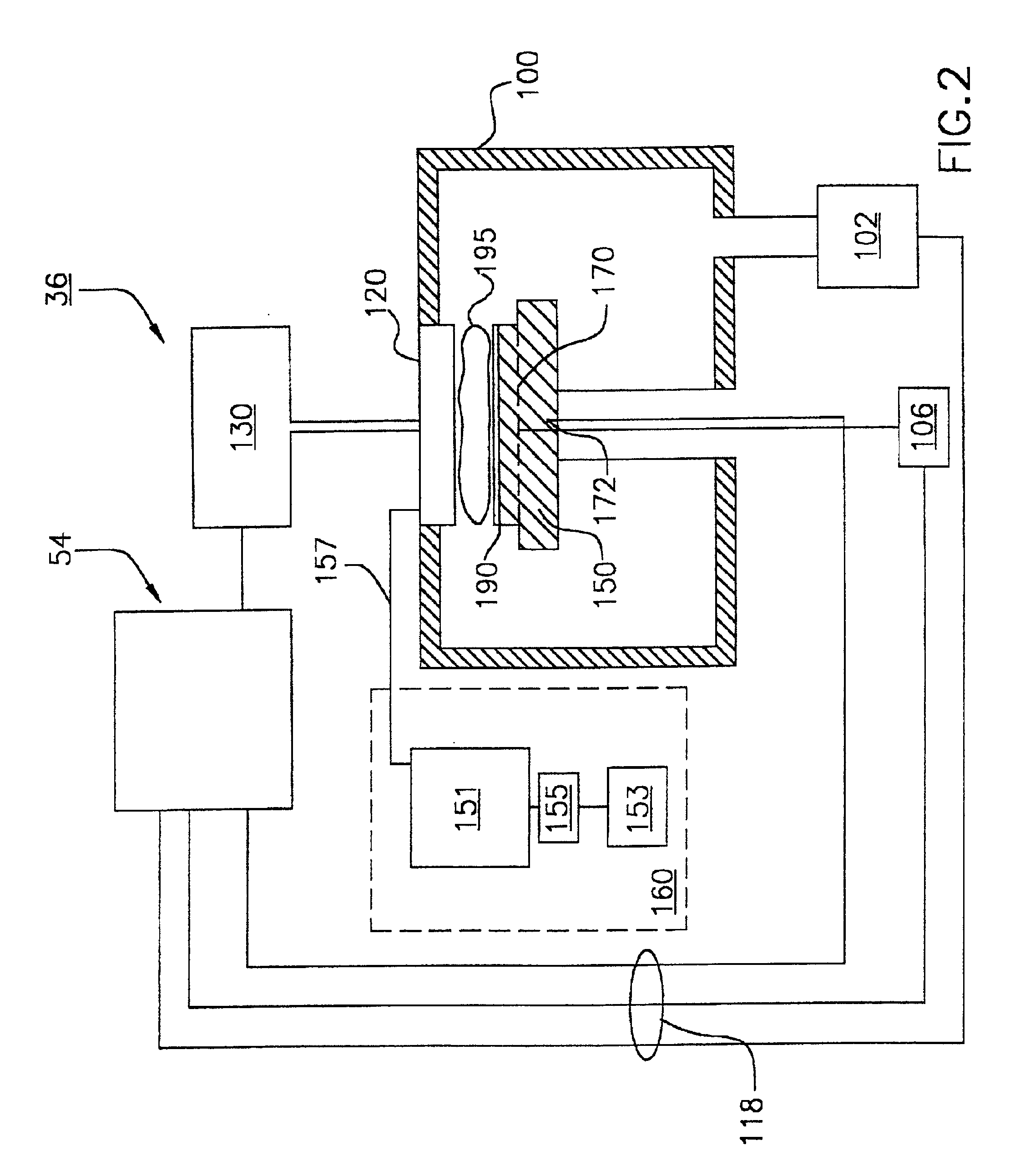
[0024]The wafer pr...


PUM

PropertyMeasurementUnit
Ratioaaaaaaaaaa

Abstract

A method of forming a titanium silicide nitride (TiSiN) layer on a substrate id described. The titanium silicide nitride (TiSiN) layer is formed by providing a substrate to a process chamber and treating the substrate with a silicon-containing gas. A titanium nitride layer is formed on the treated substrate and exposed to a silicon-containing gas. The titanium nitride (TiN) layer reacts with the silicon-containing gas to form the titanium silicide nitride (TiSiN) layer. The formation of the titanium silicide nitride (TiSiN) layer is compatible with integrated circuit fabrication processes. In one integrated circuit fabrication process, the titanium silicide nitride (TiSiN) layer may be used as a diffusion barrier for a tungsten (W) metallization process.

Description

CROSS-REFERENCE TO RELATED APPLICATIONS[0001]This application is a continuation-in-part of co-pending U.S. patent application Ser. No. 10 / 026,378, entitled “METHOD OF TISIN DEPOSITION USING A CHEMICAL VAPOR DEPOSITION (CVD) PROCESS” and filed on Dec. 21, 2001; co-pending U.S. patent application Ser. No. 08 / 808,246, entitled “METHOD FOR CONSTRUCTING A FILM ON A SEMICONDUCTOR WAFER” and filed on Feb. 28, 1997; U.S. patent application Ser. No. 08 / 498,990, entitled “BIASED PLASMA ANNEALING OF THIN FILMS” and filed on Jul. 6, 1995 now abandoned; U.S. patent application Ser. No. 08 / 567,461, entitled “PLASMA ANNEALING OF THIN FILMS” and filed on Dec. 5, 1995 now abandoned; U.S. patent application Ser. No. 08 / 677,185, entitled “CHAMBER FOR CONSTRUCTING AN OXIDIZED FILM ON A SEMICONDUCTOR WAFER” and filed on Jul. 9, 1996 now U.S. Pat No. 6,155,198 ; U.S. patent application Ser. No. 08 / 677,218, entitled “IN-SITU CONSTRUCTION OF AN OXIDIZED FILM ON A SEMICONDUCTOR WAFER”, and filed on Jul. 9, ...

Claims


Application Information

Patent Timeline
IPC IPC(8): C23C16/56C23C16/458C23C16/48C23C16/50C23C16/509C23C16/34H01L21/02H01L21/70H01J37/32H01L21/285H01L21/768C23C16/44C23C16/455
CPCC23C16/34C23C16/4408C23C16/45565C23C16/4581C23C16/4586C23C16/481C23C16/5096C23C16/56H01J37/32174H01L21/28512H01L21/28556H01L21/76843H01L21/76856H01L21/76862H01J2237/2001H01J2237/336
Inventor CHOU, JING-PEIKAO, CHIEN-TEHLAI, CHIUKINMOSELY, RODERICK C.CHANG, MEI
Owner APPLIED MATERIALS INC
Why Eureka
Try Eureka