Evaluation device for evaluating semiconductor device
a technology of semiconductor devices and evaluation devices, applied in the direction of individual semiconductor device testing, semiconductor/solid-state device testing/measurement, instruments, etc., can solve the problems of increased failure rate of evaluation and analysis, increased failure rate etc., to reduce the size of contacts and vias, reduce the size of semiconductor devices, and increase the integration rate
- Summary
- Abstract
- Description
- Claims
- Application Information
AI Technical Summary
Benefits of technology
Problems solved by technology
Method used
Image

Examples
first embodiment
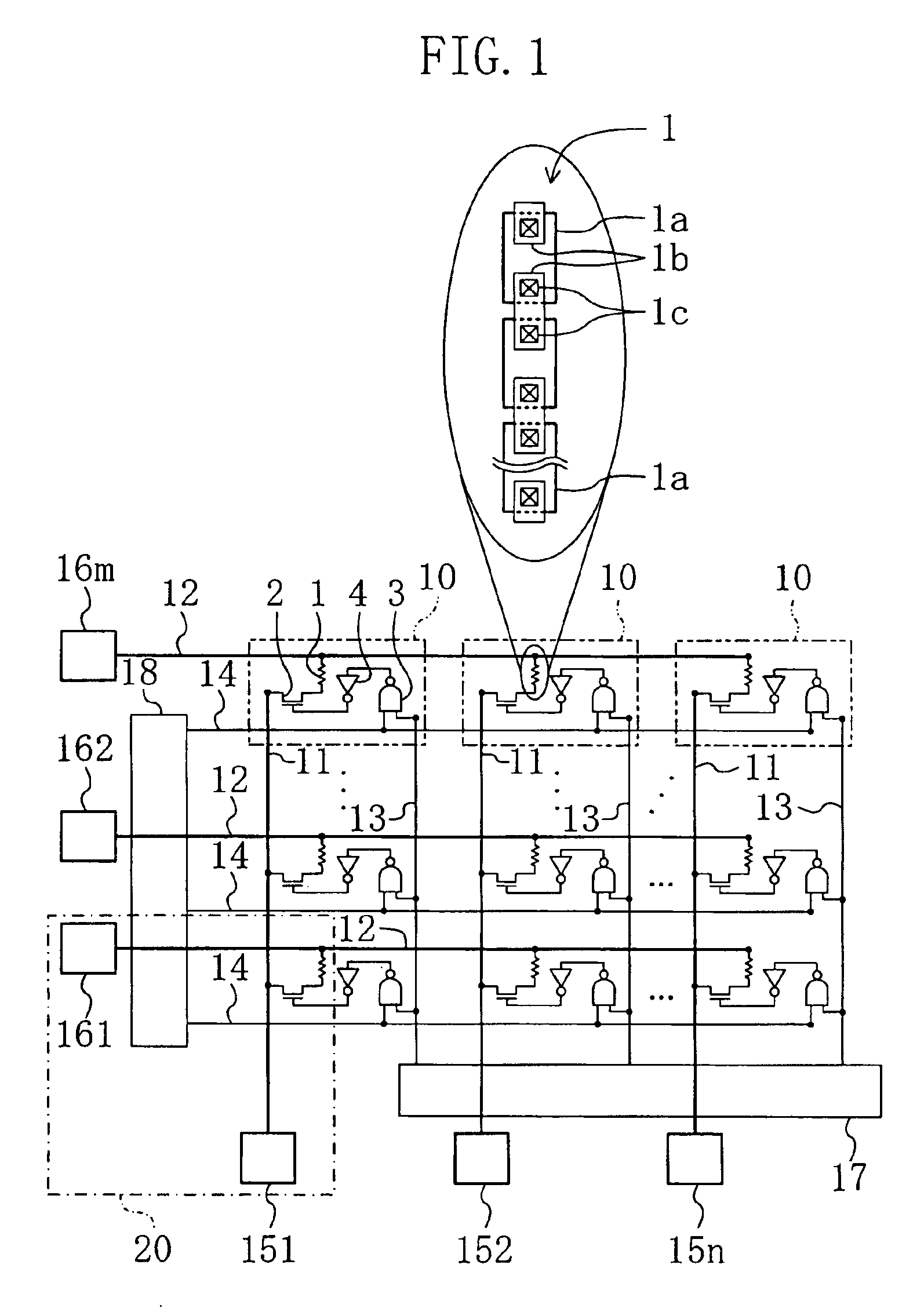
[0076](First Embodiment)
[0077]A first embodiment of the present invention will be described with reference to the accompanying drawings.
[0078]FIG. 1 is a circuit diagram illustrating the circuit configuration of an evaluation device for evaluating a semiconductor device according to the first embodiment of the present invention.
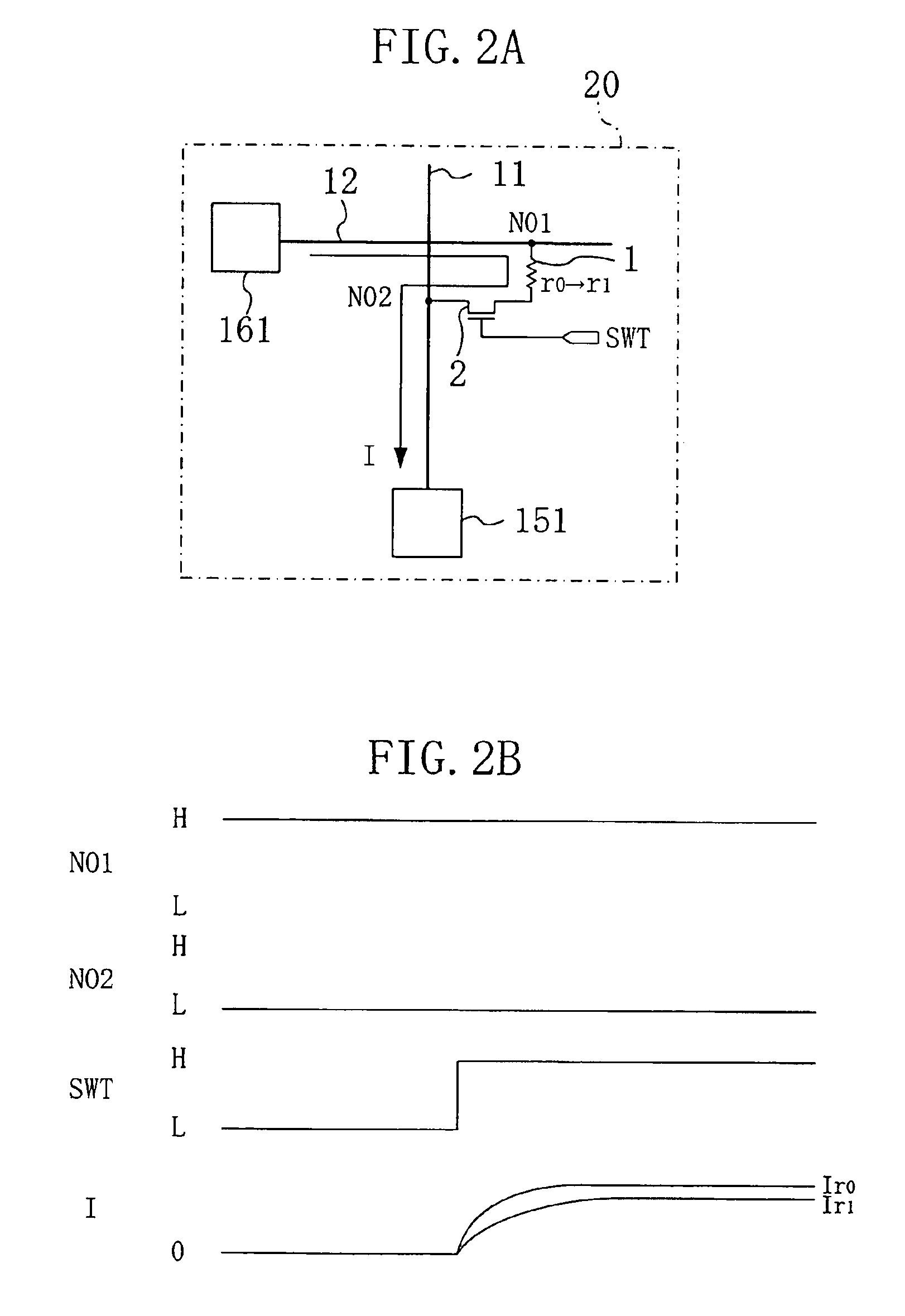
[0079]As shown in FIG. 1, the semiconductor device evaluation device of the first embodiment is, for example, a so-called “TEG (test element group)” formed in part of a semiconductor wafer made of silicon (Si). In the semiconductor device evaluation device, a plurality of unit circuits 10 each including a resistance element 1 to be evaluated and a switching transistor 2 made of an n-type MOSFET with a source connected to a column power supply line 11 and a drain connected to one terminal of the resistance element 1 are arranged in a matrix.
[0080]In each of the unit circuits 10, the other terminal of the resistance element 1 is connected to a row power supply ...
second embodiment
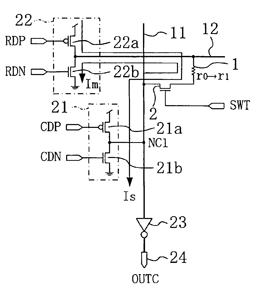
[0095](Second Embodiment)
[0096]Hereinafter, a second embodiment of the present invention will be described with reference to the accompanying drawings.
[0097]FIG. 3 is a circuit diagram illustrating a circuit configuration of a unit circuit of an evaluation device for evaluating a semiconductor device according to the second embodiment of the present invention. In FIG. 3, each member also shown in FIG. 1 is identified by the same reference numeral and therefore description thereof will be omitted.
[0098]The evaluation device for evaluating a semiconductor device according to the second embodiment has, in addition to the configuration of the first embodiment, a configuration which allows evaluation of a resistance value of a resistance element in a short time.
[0099]As shown in FIG. 3, the semiconductor device evaluation device of the second embodiment includes, instead of the column pads 15n and the row pads 16m, a column driver circuit 21 as a first circuit of which an output terminal...
third embodiment
[0118](Third Embodiment)
[0119]Hereinafter, a third embodiment of the present invention will be described with reference to the accompanying drawings.
[0120]FIG. 6 is a circuit diagram illustrating a circuit configuration of a unit circuit of an evaluation device for evaluating a semiconductor device according to a third embodiment of the present invention. In FIG. 6, each member also shown in FIG. 3 is identified by the same reference numeral and therefore description thereof will be omitted.
[0121]The semiconductor device evaluation device of the third embodiment has, in addition to the configuration of the second embodiment, a configuration which allows application of a stress current in a reverse direction.
[0122]As shown in FIG. 6, the third embodiment is characterized in that a second resistance element 27 is connected between the source of the switching transistor 2 and the column power supply line 11. In this case, the second resistance element 27 is preferably a via chain havin...
PUM
 Abstract
Description
Claims
Application Information
 - R&D
- Intellectual Property
- Life Sciences
- Materials
- Tech Scout
- Unparalleled Data Quality
- Higher Quality Content
- 60% Fewer Hallucinations
Browse by: Latest US Patents, China's latest patents, Technical Efficacy Thesaurus, Application Domain, Technology Topic, Popular Technical Reports.
© 2025 PatSnap. All rights reserved.Legal|Privacy policy|Modern Slavery Act Transparency Statement|Sitemap|About US| Contact US: help@patsnap.com