Organic electroluminescent device

a technology of electroluminescent devices and electroluminescent devices, which is applied in the direction of discharge tube luminescent screens, other domestic articles, natural mineral layered products, etc., can solve the problems of unstable light emission, device production using bcp tends to suffer from current leakage, and bcp is prone to crystallization, etc., to achieve stable light emission, high luminescent efficiency, and high luminance

Inactive Publication Date: 2005-07-26
SANYO ELECTRIC CO LTD
View PDF3 Cites 3 Cited by
  • Summary
  • Abstract
  • Description
  • Claims
  • Application Information

AI Technical Summary

Benefits of technology

[0018]It is an object of the present invention to provide an organic electroluminescent device capable of stably emitting light with high luminance and high luminescent efficiency.
[0021]The presence of the hole blocking layer increases the energy barrier between the luminescent layer and the hole blocking layer. Therefore, holes can be prevented from being injected into the electron injection electrode side from the luminescent layer, so that electrons and holes can efficiently be recombined in the luminescent layer. Thus, the luminance and the luminescent efficiency of the organic electroluminescent device can be improved.
[0022]Since the above ternary complex compound is stable, the organic electroluminescent device can stably emit light.
[0030]In this way, holes can be prevented from being injected into the electron transport layer from the luminescent layer, so that electrons and holes can efficiently be recombined at the luminescent layer. Therefore, the luminescent efficiency of the organic electroluminescent device can be improved.

Problems solved by technology

The BCP is however prone to crystallization with time after it is formed into a film.
Therefore, the organic EL device produced using the BCP tends to suffer from current leakage, and stable light emission is not provided.

Method used


Image

  • Organic electroluminescent device
  • Organic electroluminescent device
  • Organic electroluminescent device

Examples


examples

[0050]Organic EL devices according to Inventive Examples 1 to 4 and Comparative Example 1 were manufactured and measured for their luminescent characteristics.

##ventive examples 1 to 4

Inventive Examples 1 to 4

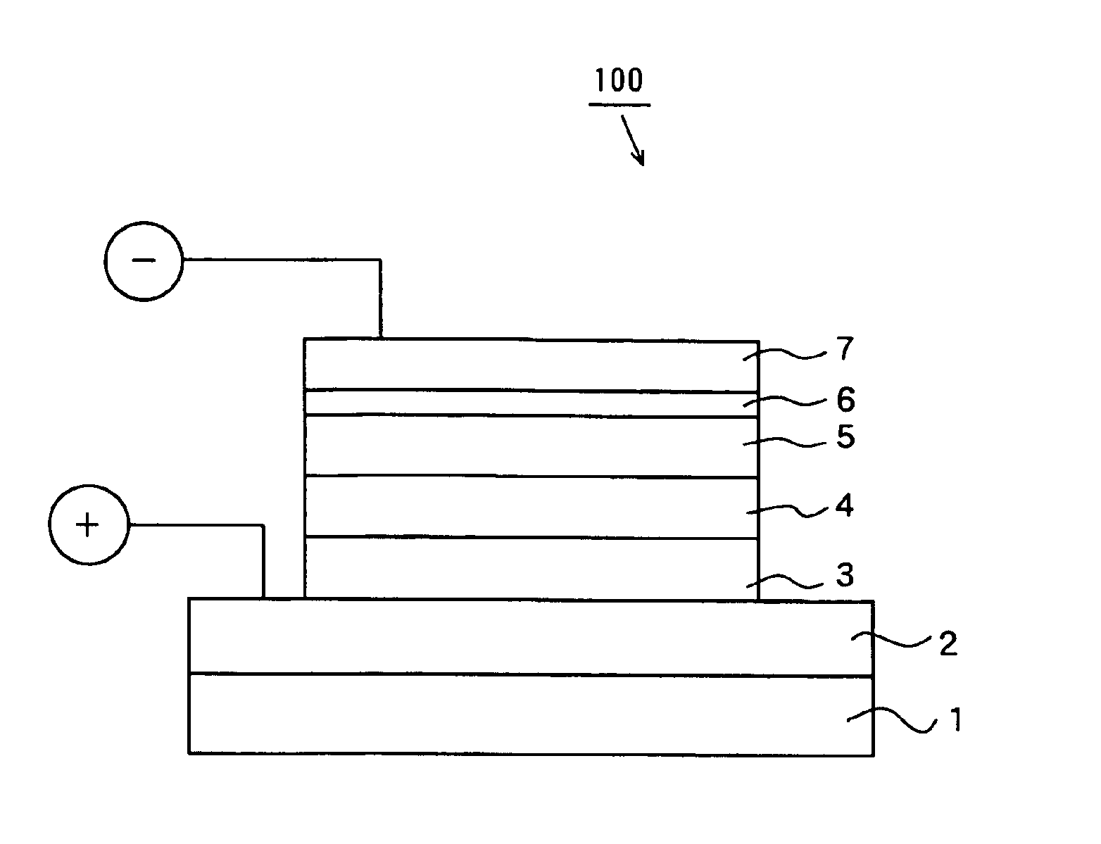
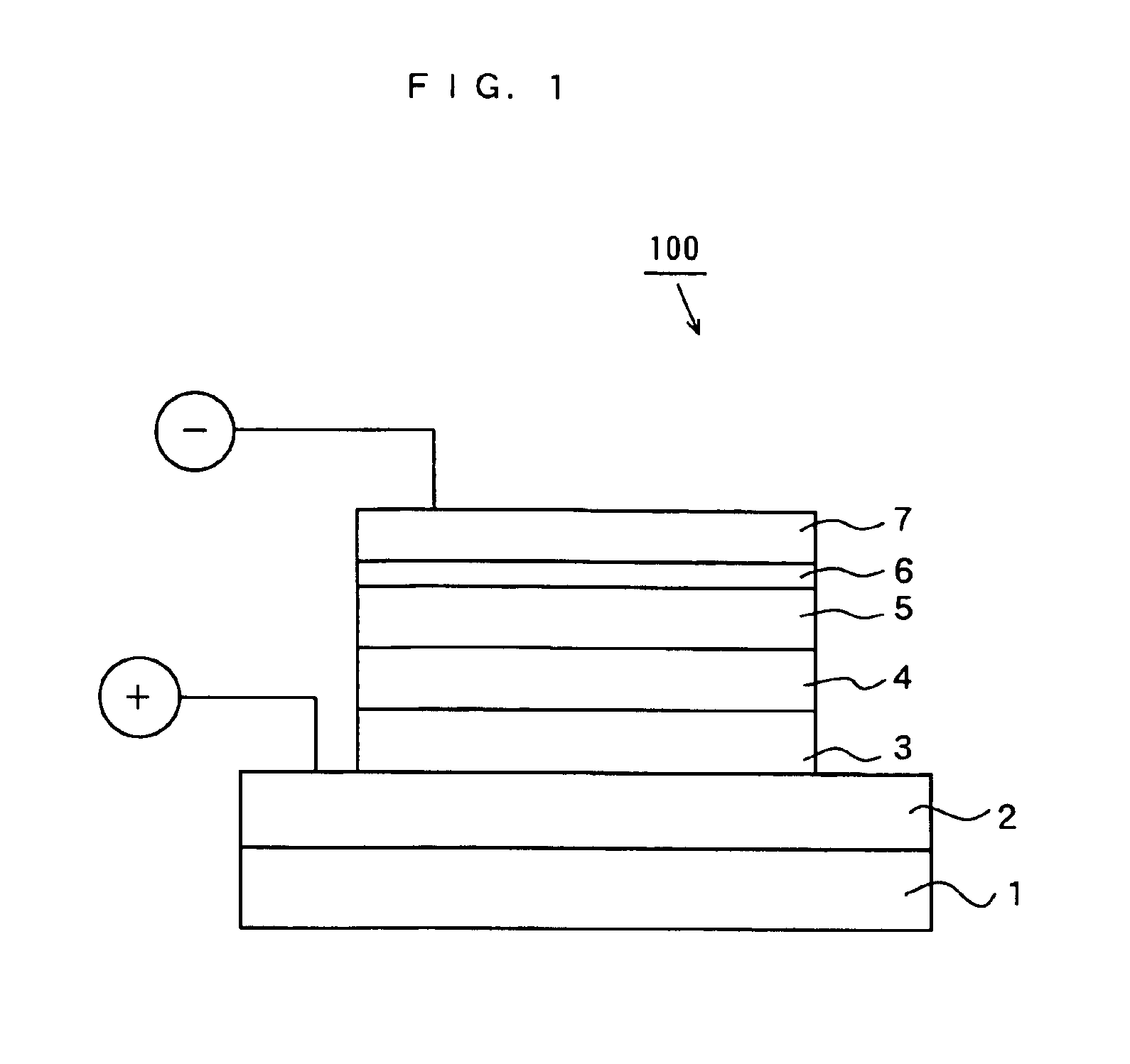
[0051]In Inventive Examples 1 to 4, such an organic EL device was used that a hole injection electrode (anode) 2, a hole transport layer 3, a luminescent layer 4, a hole blocking layer 5, an electron transport layer 6 and an electron injection electrode (cathode) 7 was stacked in this order on a glass substrate 1.

[0052]In this case, the hole injection electrode 2 in the organic EL device is as thick as 1000 Å and composed of indium-tin oxide (ITO). The hole transport layer 3 is as thick as 500 Å and composed of N,N′-di(naphthalen-1-yl)-N,N′-diphenyl-benzidine) (hereinafter referred to as “NPB”) having a molecular structure represented by the following formula (7):

[0053]The luminescent layer 4 is as thick as 100 Å and it contains 4,4′-bis(carbazol-9-yl)-biphenyl (hereinafter referred to as “CBP”) having a molecular structure represented by the following formula (8) as a host material and tris(2-phenylpyridine)iridium (hereinafter referred to as “Ir(ppy)3”) h...


PUM

PropertyMeasurementUnit
ionization potentialaaaaaaaaaa
luminanceaaaaaaaaaa

Abstract

In an organic EL device, a hole injection electrode is formed on a glass substrate, and a hole transport layer, a luminescent layer, a hole blocking layer, an electron transport layer, and an electron injection electrode are formed in this order on the glass substrate. The hole blocking layer includes a ternary complex compound including two quinolinol derivatives, a group IIIB element, and a halogen element or a phenol derivative.

Description

BACKGROUND OF THE INVENTION[0001]1. Field of the Invention[0002]The present invention relates to organic electroluminescent devices.[0003]2. Description of the Background Art[0004]Organic electroluminescence devices (hereinafter referred to as organic EL devices) are expected as new self-light emitting devices. An organic EL device has a stacked layered structure that a carrier transport layer (an electron transport layer or a hole transport layer) and a luminescent layer are formed between a hole injection electrode and an electron injection electrode.[0005]Electrode materials having a large work function such as gold or ITO (indium-tin oxide) are employed for the hole injection electrode, while those having a small work function such as Mg (magnesium) or Li (lithium) are employed for the electron injection electrode.[0006]Organic materials are employed for the hole transport layer, the luminescent layer and the electron transport layer. Materials having the property of a p-type se...

Claims


Application Information

Patent Timeline
Patent Type & Authority Patents(United States)
IPC IPC(8): H01L51/50H01L51/05H01L51/30H01L51/00
CPCH01L51/5096H01L51/0085H01L51/5048H01L51/005H01L51/0059H01L51/0062H01L51/0077H01L51/0081Y10S428/917H10K85/60H10K85/649H10K85/631H10K85/30H10K85/324H10K85/342H10K50/14H10K50/18
Inventor HAMADA, YUJIMATSUSUE, NORIYUKI
Owner SANYO ELECTRIC CO LTD
Why Eureka
Try Eureka