
High frequency switch

a high-frequency switch and switch technology, applied in the direction of high-frequency circuit adaptation, high-frequency circuit adaptation, printed circuit non-printed electric components association, etc., can solve the problems of preventing the sufficient downsizing of the high-frequency switch and blocking integration

Inactive Publication Date: 2005-07-12
PANASONIC CORP
View PDF12 Cites 58 Cited by
  • Summary
  • Abstract
  • Description
  • Claims
  • Application Information

AI Technical Summary

Benefits of technology

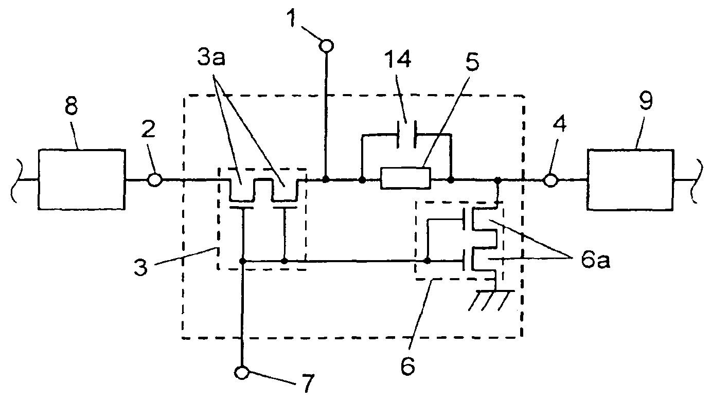
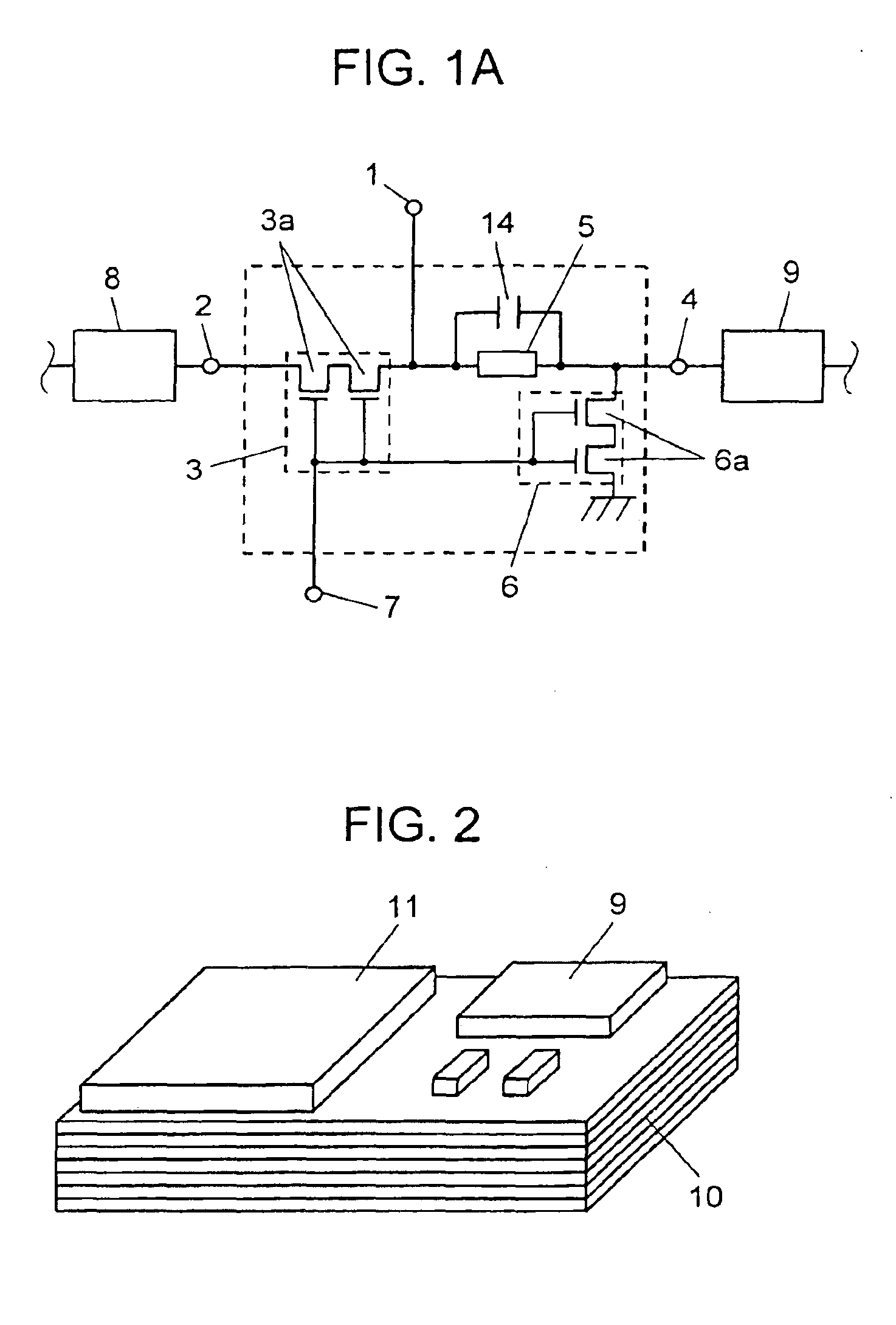
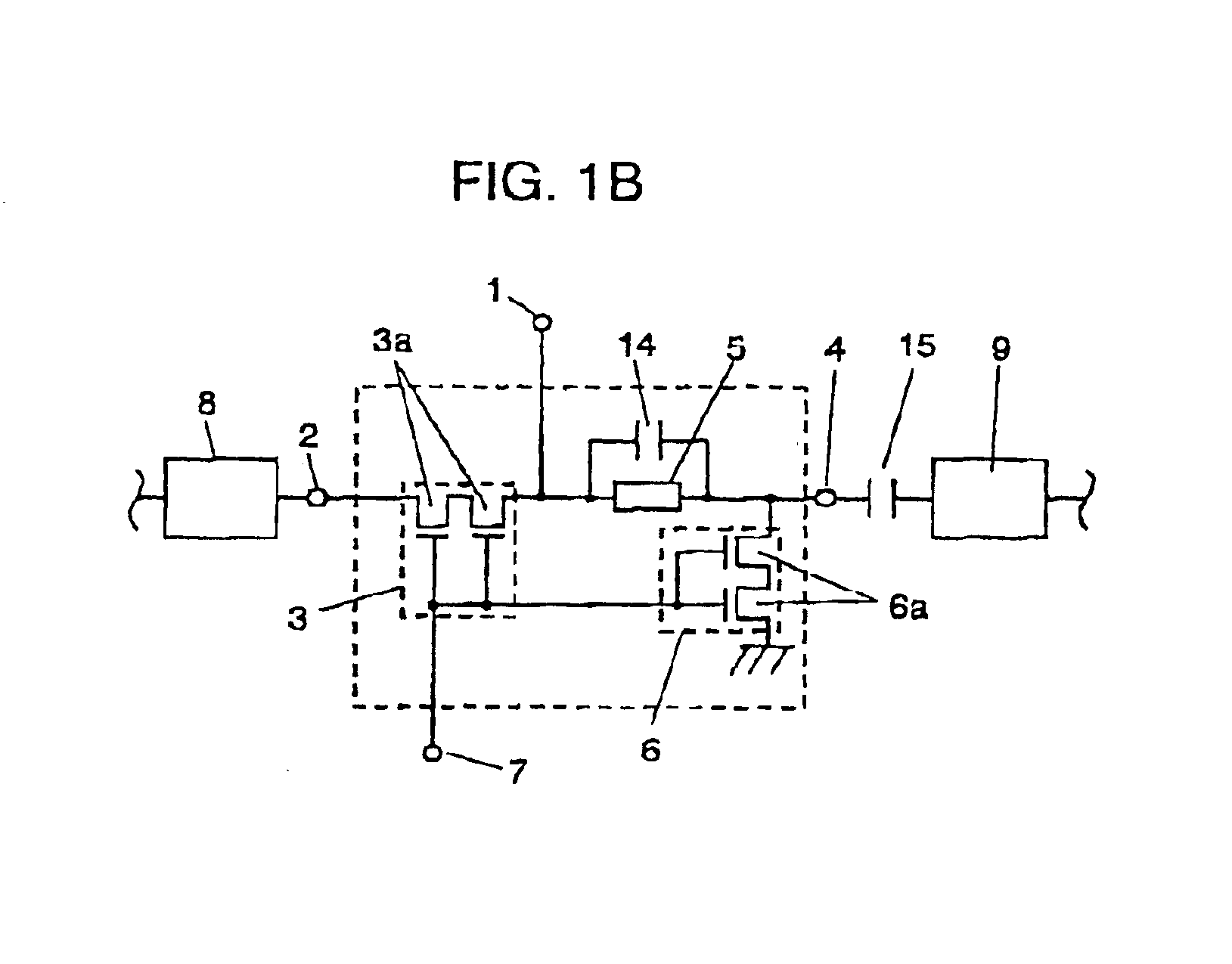
[0007]The present invention offers a high frequency switch which includes a first FET switch connected between an input / output (I / O) port and a transmission port, a second FET switch whose one end is connected between the I / O port and reception port and the other end is grounded, a control port controlling ON and OFF of the first and second FET switches, and a parallel unit of a strip line and capacitor. The electrical length of this parallel unit connected between one end of the second FET switch and I / O port is equivalent to about ¼ wavelength of the high frequency signal input from the transmission port.

Problems solved by technology

This hinders sufficient downsizing of the high frequency switch and blocks integration.

Method used


Image

  • High frequency switch
  • High frequency switch
  • High frequency switch

Examples


first exemplary embodiment

[0012]FIG. 1A is a circuit diagram of a high frequency switch employed in an RF circuit of a mobile phone. This high frequency switch basically includes first field-effect transistor switch (FET switch) 3 connected between input / output (I / O) port 1 and transmission port 2, strip line 5 connected between I / O port 1 and reception port 4, second field-effect transistor switch (FET switch) 6 connected between strip line 5 to the side of reception port 4 and a ground, and control port 7 which controls ON and OFF of the above two FET switches 3 and 6.

[0013]During transmission, a control voltage is applied from control port 7 to two FET switches 3 and 6 so as to turn on two FET switches 3 and 6. The electrical length of strip line 5 is set to about ¼ wavelength of the transmission signal so as to ground strip line 5 via second FET switch 6. This keeps the side of reception port 4, as seen from I / O port 1, open, allowing transmission signals input from transmission port 2 to flow efficientl...

second exemplary embodiment

[0026]The high frequency switch described in the first exemplary embodiment refers to an SPDT-type high frequency switch circuit in which transmission port 2 and reception port 4 are generally switched as required against one I / O port 1.

[0027]FIG. 3 is a combined high frequency switch for multiple bands in which two or more types of transmission and receiving signals in different frequency bands are handled by connecting diplexer 13 to I / O port of two high frequency switches 12. In this case, the circuit configuration becomes more complex, and FET switches 3 and 6 and other chip components such as capacitors and inductors need to be densely mounted on the top face of multilayer board 10. The integration achieved by the present invention, as described, is thus extremely effective for saving mounting space on the top face of multilayer board 10.

[0028]In the present invention, a strip line is provided between the second FET switch whose one end is connected between the I / O port and rec...


PUM


Abstract

A high frequency switch configured particularly with FET switches. One end of second FET switch is connected between I / O port and reception port and the other end is ground. A parallel unit of strip line and capacitor is connected between second FET switch and I / O port. This parallel unit has the electrical length equivalent to ¼ wavelength of the high frequency signal input from transmission port.

Description

BACKGROUND OF THE INVENTION[0001]1. Field of the Invention[0002]The present invention relates to high frequency switches typically used in the RF circuits of mobile phones.[0003]2. Background Art[0004]A known structure of a high frequency switch used in an RF circuit of high frequency wireless apparatuses such as mobile phones is to mount a PIN diode on a multilayer board with a built-in strip line. (For example, refer to Japanese Laid-open Patent No. H8-97743 (pp. 3-4, FIGS. 1, 2, and 3).)[0005]Ever greater integration of the high frequency switch and other high frequency components such as high frequency filters and amplifiers disposed around the high frequency switch is being seen. To allow integration, high frequency switches mounted on the multilayer board need to be downsized to secure extra space for mounting other high frequency components. One currently proposed method for downsizing high frequency switches using a PIN diode is the use of a field-effect transistor switch (F...

Claims


Application Information

Patent Timeline
IPC IPC(8): H03K17/687H03K17/693H04B1/44H04B1/48H01P1/15H01P1/10H05K1/00H05K1/18H05K1/16H05K1/02
CPCH01P1/15H03K17/6871H03K17/693H04B1/48H05K1/0237H05K1/0298H05K1/162H05K1/181
Inventor KUSHITANI, HIROSHINAGATA, YASUSHIYASUHO, TAKEO
Owner PANASONIC CORP
Learn More