Method and system of calibrating the control delay time
- Summary
- Abstract
- Description
- Claims
- Application Information
AI Technical Summary
Benefits of technology
Problems solved by technology
Method used
Image
Examples
Embodiment Construction
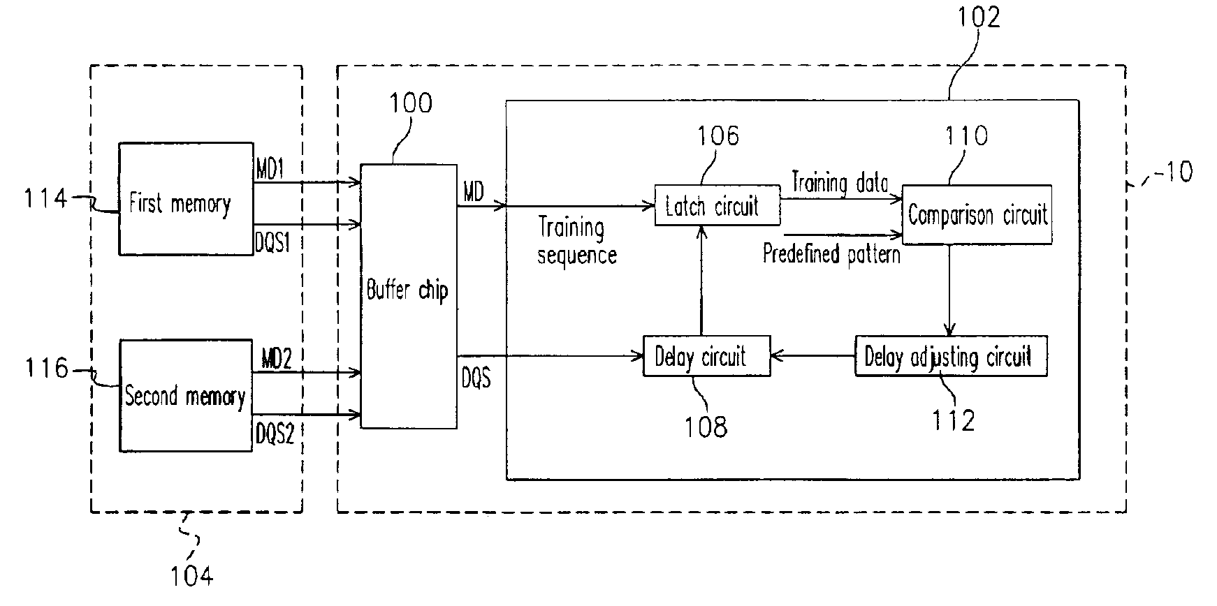
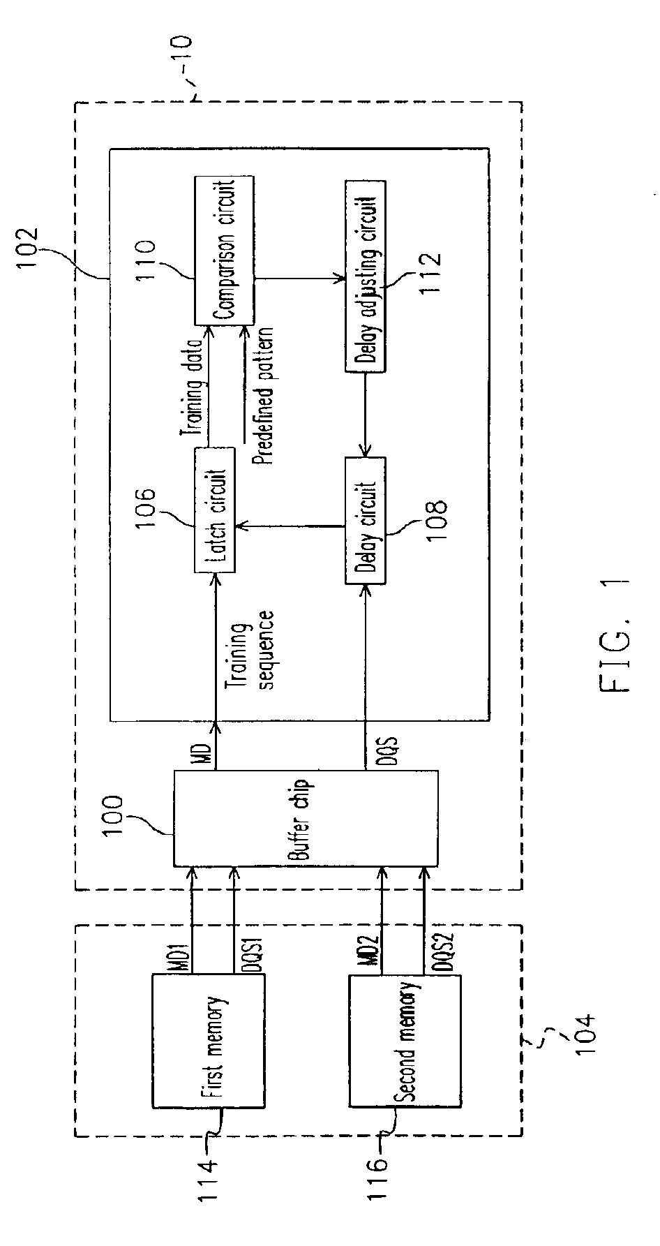
[0016]FIG. 1 schematically shows a block diagram of a system of calibrating the control delay time of a preferred embodiment according to the present invention. As shown in the diagram, the system of calibrating the control delay time 10 comprises a buffer chip 100 and a control chip 102 (e.g. a north bridge chip). Wherein, the buffer chip 100 connects to the control chip 102 and a memory 104. The buffer chip 100 mentioned above may be integrated into the memory 104 or separated from the memory 104 as designed. The control chip 102 comprises a latch circuit 106, a delay circuit 108, a comparison circuit 110 and a delay adjusting circuit 112.
[0017]Herein, in order to adapt to the control chip 102 for rapidly reading the data from memory, so as to improve the processing speed and the performance of the computer system. The memory 104 comprises a first memory 114 and a second memory 116. The DDR SDRAM is used as the first memory 114 and the second memory 116 to access data. That is, tw...
PUM
 Abstract
Description
Claims
Application Information
 - R&D
- Intellectual Property
- Life Sciences
- Materials
- Tech Scout
- Unparalleled Data Quality
- Higher Quality Content
- 60% Fewer Hallucinations
Browse by: Latest US Patents, China's latest patents, Technical Efficacy Thesaurus, Application Domain, Technology Topic, Popular Technical Reports.
© 2025 PatSnap. All rights reserved.Legal|Privacy policy|Modern Slavery Act Transparency Statement|Sitemap|About US| Contact US: help@patsnap.com


