Piezoelectric element, actuator, and inkjet head
a technology of actuators and piezoelectric elements, applied in piezoelectric/electrostrictive/magnetostrictive devices, piezoelectric/electrostriction/magnetostriction machines, printing, etc., can solve the problems of difficult to obtain good characteristics, large size of 30 mm30 mm, and high cost of single crystal substrates, etc. good piezoelectric characteristics
- Summary
- Abstract
- Description
- Claims
- Application Information
AI Technical Summary
Benefits of technology
Problems solved by technology
Method used
Image

Examples
first embodiment
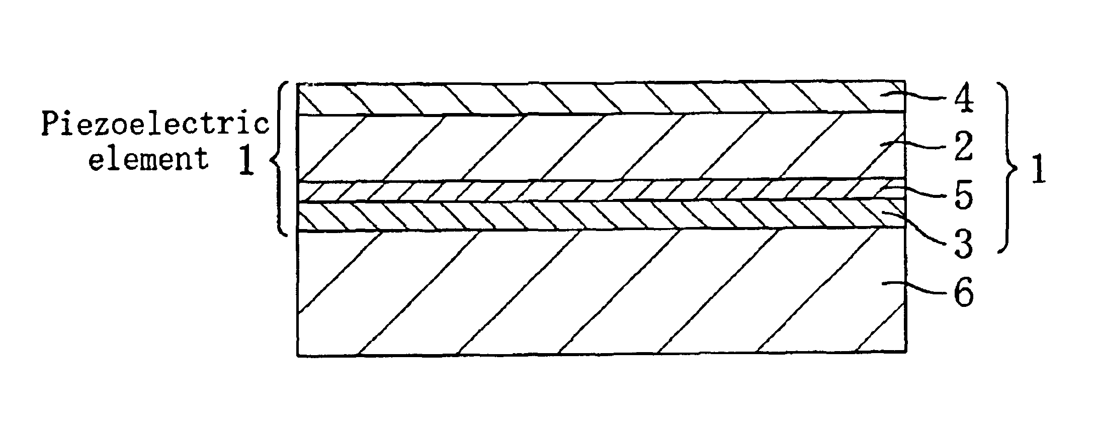
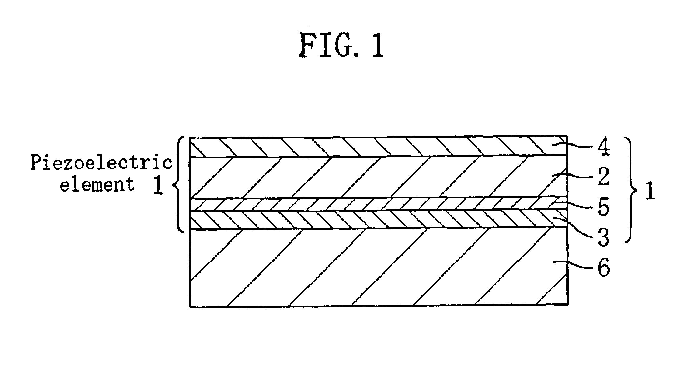
[0051]FIG. 1 is a cross-sectional view illustrating a structure of a piezoelectric element 1 according to the first embodiment of the present invention. The piezoelectric element 1 of the present embodiment includes a piezoelectric film 2 having a thickness of 0.1 μm to 50 μm, a pair of electrodes (a lower electrode 3 and an upper electrode 4) arranged with the piezoelectric film 2 being interposed therebetween, and a base film 5 having a thickness of about 50 nm to 200 nm between the piezoelectric film 2 and the lower electrode 3. The piezoelectric element 1, as a whole, is provided on a substrate 6, which may be a stainless steel substrate (polycrystalline), a heat-resistant glass substrate (amorphous), a silicon substrate (single crystal), etc.
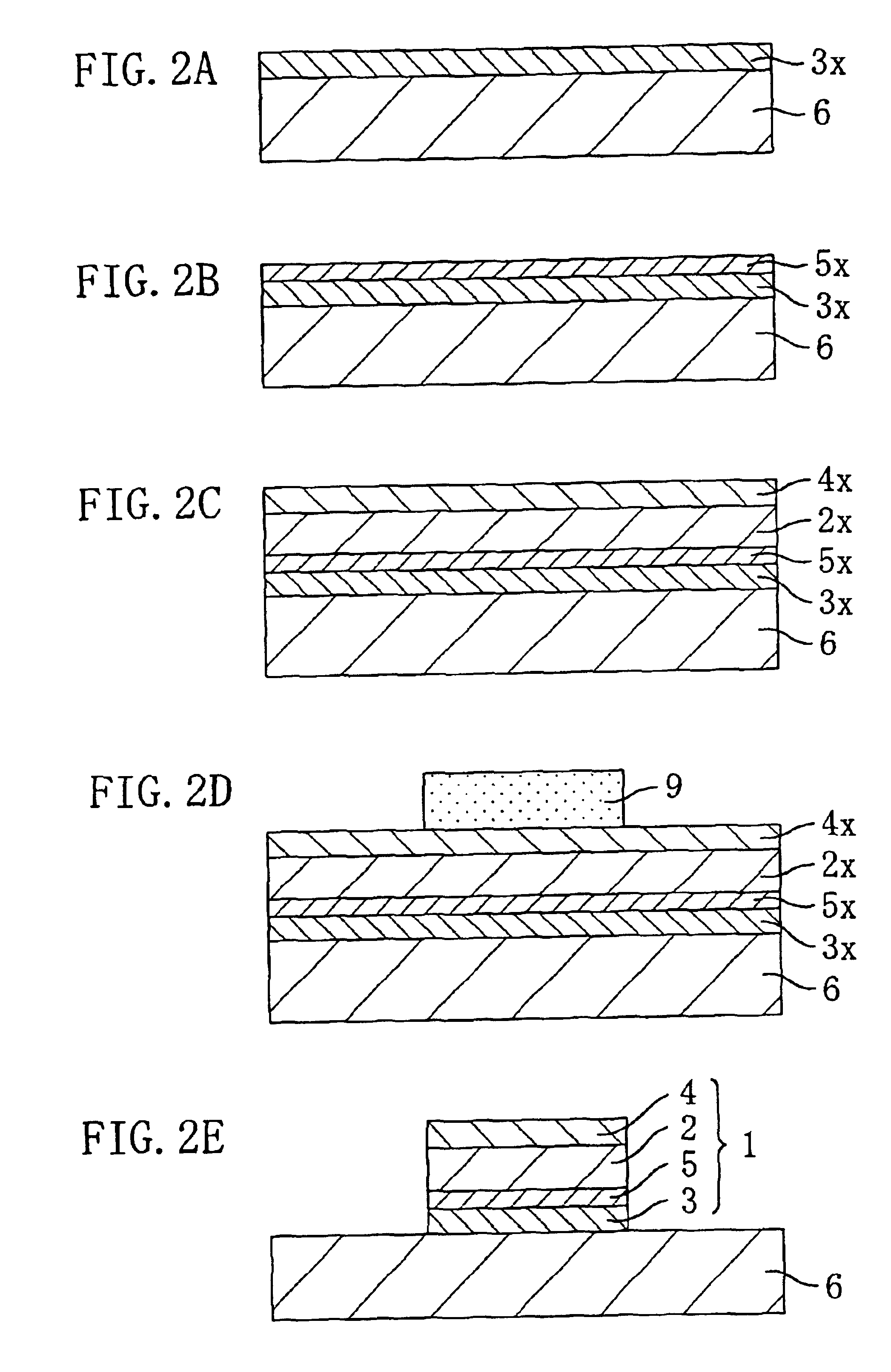
[0052]FIG. 2A to FIG. 2E are cross-sectional views illustrating the steps in a method for manufacturing a thin-film semiconductor element of the present embodiment.
[0053]First, in the step of FIG. 2A, a Pt film 3x to be the lower electrode ...
examples
[0066]The following specific samples were subjected to a piezoelectric constant measurement in order to confirm the effects of the present embodiment. Samples having the structure as illustrated in FIG. 1 were produced while using various materials for the substrate 6 and eight values of 25 nm, 50 nm, 75 nm, 100 nm, 125 nm, 150 nm, 175 nm and 200 nm for the thickness of the base film 5 made of PLT, so as to determine changes in the piezoelectric constant d31 in response to changes in the thickness of the base film.
[0067]An MgO single crystal substrate, a silicon single crystal substrate, a stainless steel substrate (polycrystalline), a polysilicon substrate, a heat-resistant glass substrate (amorphous), a titanium substrate (polycrystalline), an iron plate (polycrystalline), a copper plate (polycrystalline), and a nickel plate (polycrystalline) were used as the substrate 6.
[0068]Note that the lower electrode 3 is a Pt film having a thickness of 100 nm, the base film 5 is a PLT film ...
second embodiment
[0109]FIG. 9A to FIG. 9D are cross-sectional views illustrating various structures of a piezoelectric actuator according to the second embodiment of the present invention.
[0110]The actuator of the present embodiment includes, as basic components, the piezoelectric element 1, a reinforcement member 14 made of a synthetic resin and provided so as to hold the piezoelectric element 1, a fixed portion 15 for supporting the reinforcement member 14, an upper electrode extraction line 16 filling a through hole 17 formed in the reinforcement member 14 so as to be connected to the upper electrode 4 of the piezoelectric element 1, and an object 18 to be driven by the piezoelectric element 1. Moreover, the reinforcement member 14 connects the fixed portion 15, the object 18 and the piezoelectric element 1 together, and thus includes a portion that functions as a moving member and a portion that functions as a fixed member.
[0111]The piezoelectric element 1 has a structure as described above in t...
PUM
| Property | Measurement | Unit |
|---|---|---|
| thickness | aaaaa | aaaaa |
| size | aaaaa | aaaaa |
| thickness | aaaaa | aaaaa |
Abstract
Description
Claims
Application Information
 - R&D
- Intellectual Property
- Life Sciences
- Materials
- Tech Scout
- Unparalleled Data Quality
- Higher Quality Content
- 60% Fewer Hallucinations
Browse by: Latest US Patents, China's latest patents, Technical Efficacy Thesaurus, Application Domain, Technology Topic, Popular Technical Reports.
© 2025 PatSnap. All rights reserved.Legal|Privacy policy|Modern Slavery Act Transparency Statement|Sitemap|About US| Contact US: help@patsnap.com