Chip scale packages manufactured at wafer level

a technology of wafers and scales, applied in the direction of semiconductor devices, semiconductor/solid-state device details, electrical devices, etc., to achieve the effect of improving the integrity of the interfa

Inactive Publication Date: 2005-06-07
SAMSUNG ELECTRONICS CO LTD
View PDF36 Cites 18 Cited by
  • Summary
  • Abstract
  • Description
  • Claims
  • Application Information

AI Technical Summary

Benefits of technology

[0007]In accordance with the present invention, a chip scale package (CSP) is manufactured at wafer-level. The CSP includes a conductor layer for redistribution of the chip pads on a semiconductor chip, one or two insulation layers and solder bumps which function as the terminals of the CSP and are interconnected to respective chip pads by the conductor layer. In one embodiment, the conductor layer is formed directly on the surface or passivation la

Problems solved by technology

However, most of the newly developed CSPs have several drawbacks in the areas of product reliability, process reliabil

Method used


Image

  • Chip scale packages manufactured at wafer level
  • Chip scale packages manufactured at wafer level
  • Chip scale packages manufactured at wafer level

Examples


Embodiment Construction

[0036]The present invention provides CSPs that include several features that can improve reliability of the packages, and a wafer-level manufacturing method for the CSPs.

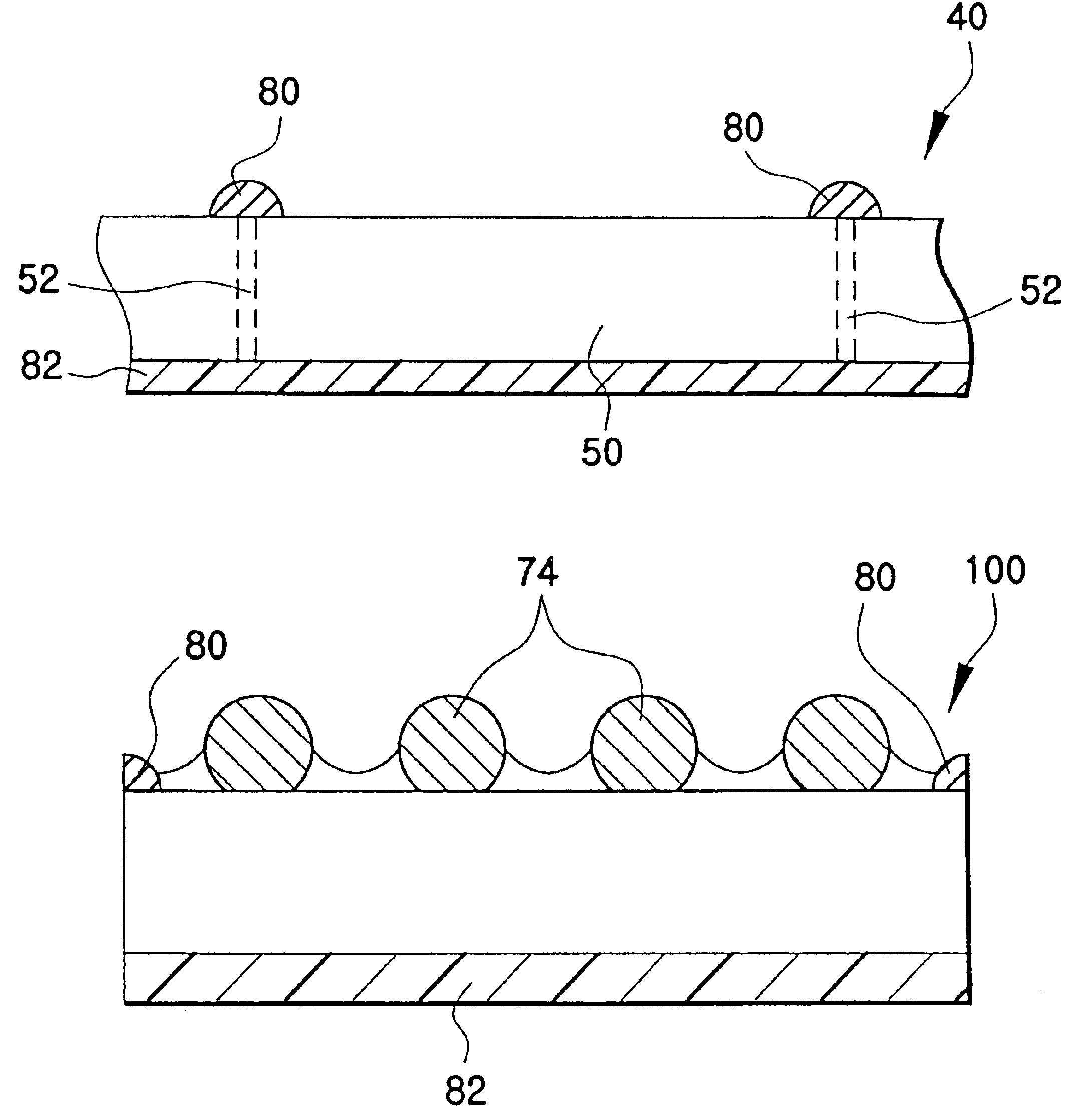
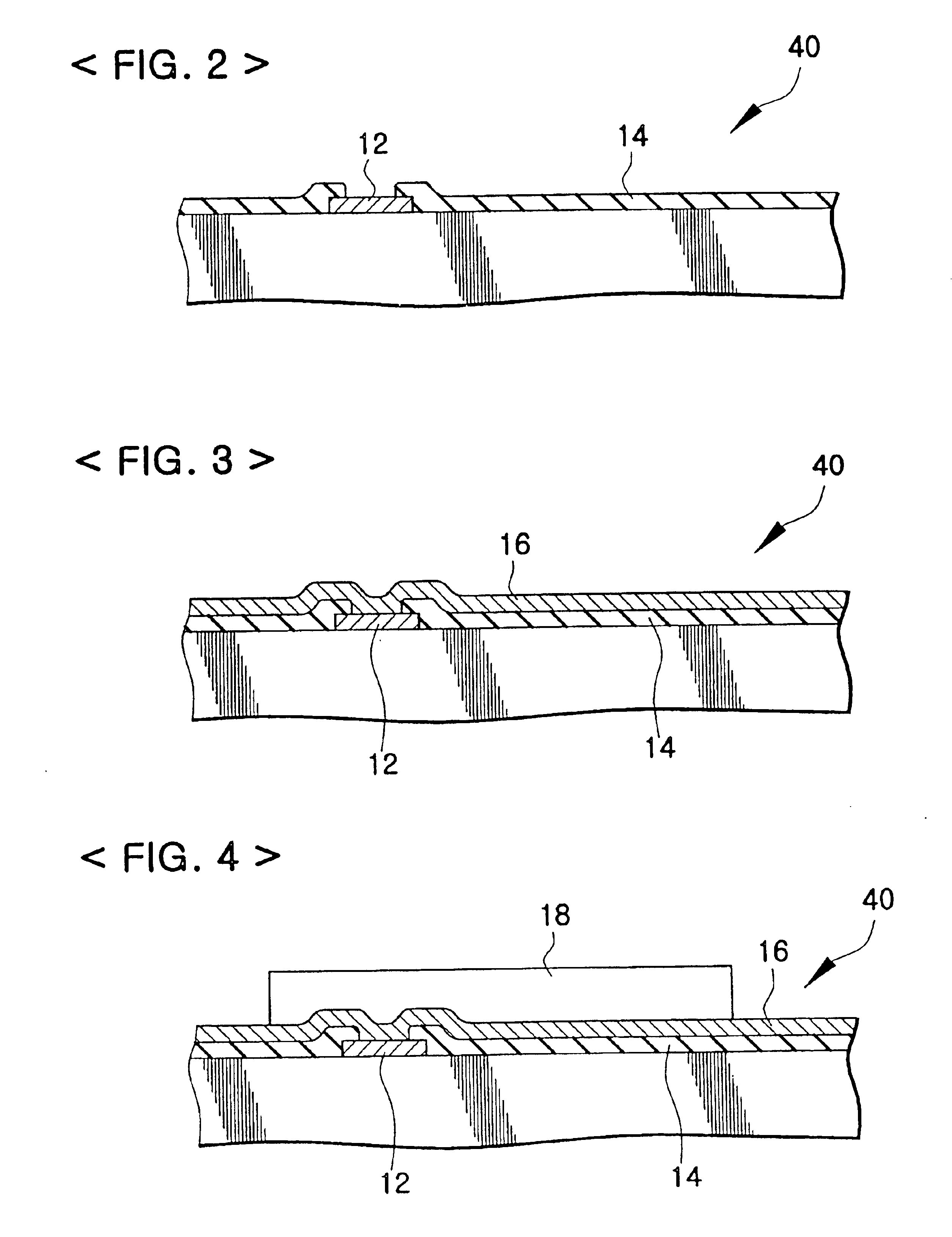
[0037]FIGS. 2 to 14 illustrate a CSP and a method for manufacturing the CSP in accordance with an embodiment of the present invention. Particularly, FIG. 14 shows a partial cross-sectional view of the CSP.

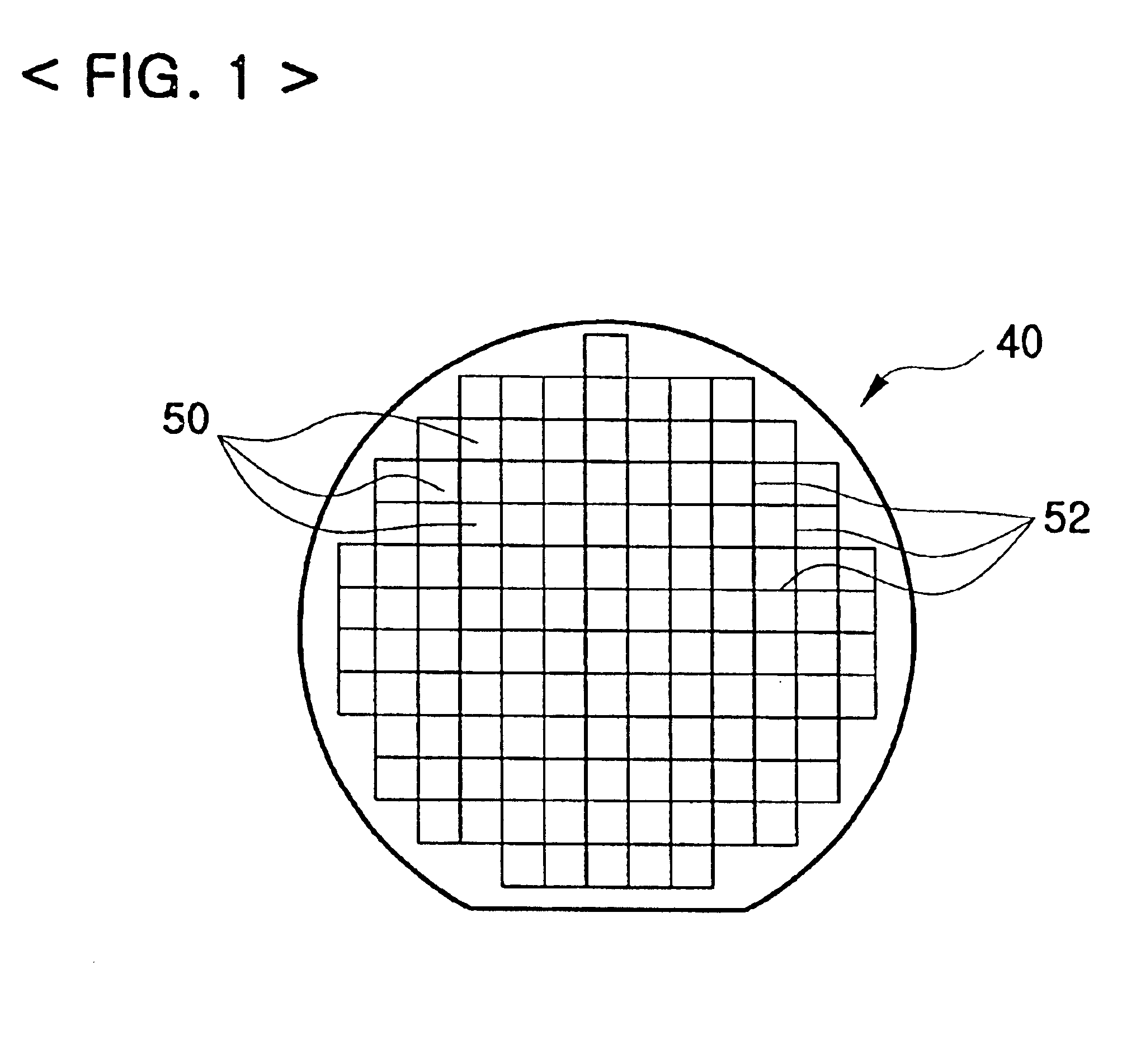
[0038]As shown in FIG. 1, manufacturing of the CSP in FIG. 14 begins with a semiconductor wafer 40 having a number of semiconductor integrated circuit chips 50 and scribe lines 52 between semiconductor chips 50. FIG. 2 is a cross-sectional view of a part of semiconductor wafer 40 showing a chip pad 12 and a passivation layer 14 of a semiconductor chip 50. Chip pad 12 is one of many chip pads that connect to the circuitry (not shown) of semiconductor chip 50, and provides access for external electrical connections. Since fabrication of semiconductor wafer 40 in FIG. 1 is a well known technology, a detailed explanati...


PUM


Abstract

In accordance with the present invention, a chip scale package (CSP) is manufactured at wafer-level. The CSP includes a chip, a conductor layer for redistribution of the chip pads of the chip, one or two insulation layers and multiple bumps, which are interconnected to respective chip pads by the conductor layer and are the terminals of the CSP. In addition, in order to improve the reliability of the CSP, a reinforcing layer, an edge protection layer and a chip protection layer are provided. The reinforcing layer absorbs stress applied to the bumps when the CSP is mounted on a circuit board and used for an extended period, and extends the life of the bumps, and thus, the life of the CSP. The edge protection layer and the chip protection layer prevent external force from damaging the CSP. After forming all elements constituting the CSP on the semiconductor wafer, the semiconductor wafer is sawed to produce individual CSPs.

Description

CROSS REFERENCE TO RELATED APPLICATION[0001]This application is a divisional of, and claims priority from U.S. patent application Ser. No. 09 / 222,250, filed Dec. 28, 1998, entitled: “Chip Scale Packages And Methods For Manufacturing The Chip Scale Packages At Wafer Level”, now U.S. Pat. No. 6,187,615 which issued, Feb. 13, 2001, which in turn claims priority from Korean Patent Application Number 98-35175 filed Aug. 28, 1998.BACKGROUND[0002]1. Field of the Invention[0003]This invention relates to chip scale packages and methods for manufacturing the packages at wafer level.[0004]2. Description of Related Art[0005]Miniaturization of electronic devices, which is one of major trends in the electronics industry, has led to the development of many technologies for manufacturing small packages, especially packages that have almost the same size as semiconductor integrated circuit chips. The Joint Electronic Device Engineering Council (JEDEC) has proposed the name ‘Chip Scale Package (CSP)’...

Claims


Application Information

Patent Timeline
IPC IPC(8): H01L21/02H01L21/60H01L23/28H01L23/31H01L23/485H01L23/48H01L23/525H01L29/06
CPCH01L23/3114H01L24/11H01L24/12H01L24/94H01L23/525H01L2224/0401H01L29/0657H01L2224/0231H01L2224/13099H01L2224/274H01L2924/01013H01L2924/01022H01L2924/01029H01L2924/01074H01L2924/01075H01L2924/01078H01L2924/14H01L2924/01023H01L2924/01024H01L2924/01033H01L2924/014H01L24/02H01L24/03H01L24/05H01L24/13H01L2224/02313H01L2224/02377H01L2224/05124H01L2224/05147H01L2224/05155H01L2224/05166H01L2224/05171H01L2224/05548H01L2224/05647H01L2224/06131H01L2224/10126H01L2224/13022H01L2224/13024H01L2924/0001H01L2924/00014H01L2224/02H01L2924/013
Inventor KIM, NAM SEOGJANG, DONG HYEONKANG, SA YOONKWON, HEUNG KYU
Owner SAMSUNG ELECTRONICS CO LTD
Why Eureka
Try Eureka