Circuitry for reducing the skew between two signals

a circuit and signal technology, applied in the field of electronic circuits, can solve the problems of digital spread delay and analog spread delay, and achieve the effect of reducing the delay between signals

Inactive Publication Date: 2005-05-24
TEXAS INSTR INC
View PDF8 Cites 2 Cited by
  • Summary
  • Abstract
  • Description
  • Claims
  • Application Information

AI Technical Summary

Benefits of technology

[0012]The present invention provides significant advantages over the prior art. The variable delay circuit can provide high precision compensation for delays between two signals as determined at the input to a circuit that uses the two signals. Therefore, the variable delay circuit takes into account all sources of delay, without needing any knowledge of the sources of delay or their possible variations. Since calibration can occur as often as desired, the variable delay circuit can compensate for dynamically varying delays. The variable delay circuit is particularly well suited for use with analog RF designs which need frequent high precision calibration between signals.

Problems solved by technology

In mixed signal design, there will be digital spread delays and analog spread delays.
The spread of each cannot be easily compensated with a unique addition of digital delay.

Method used


Image

  • Circuitry for reducing the skew between two signals
  • Circuitry for reducing the skew between two signals
  • Circuitry for reducing the skew between two signals

Examples


Embodiment Construction

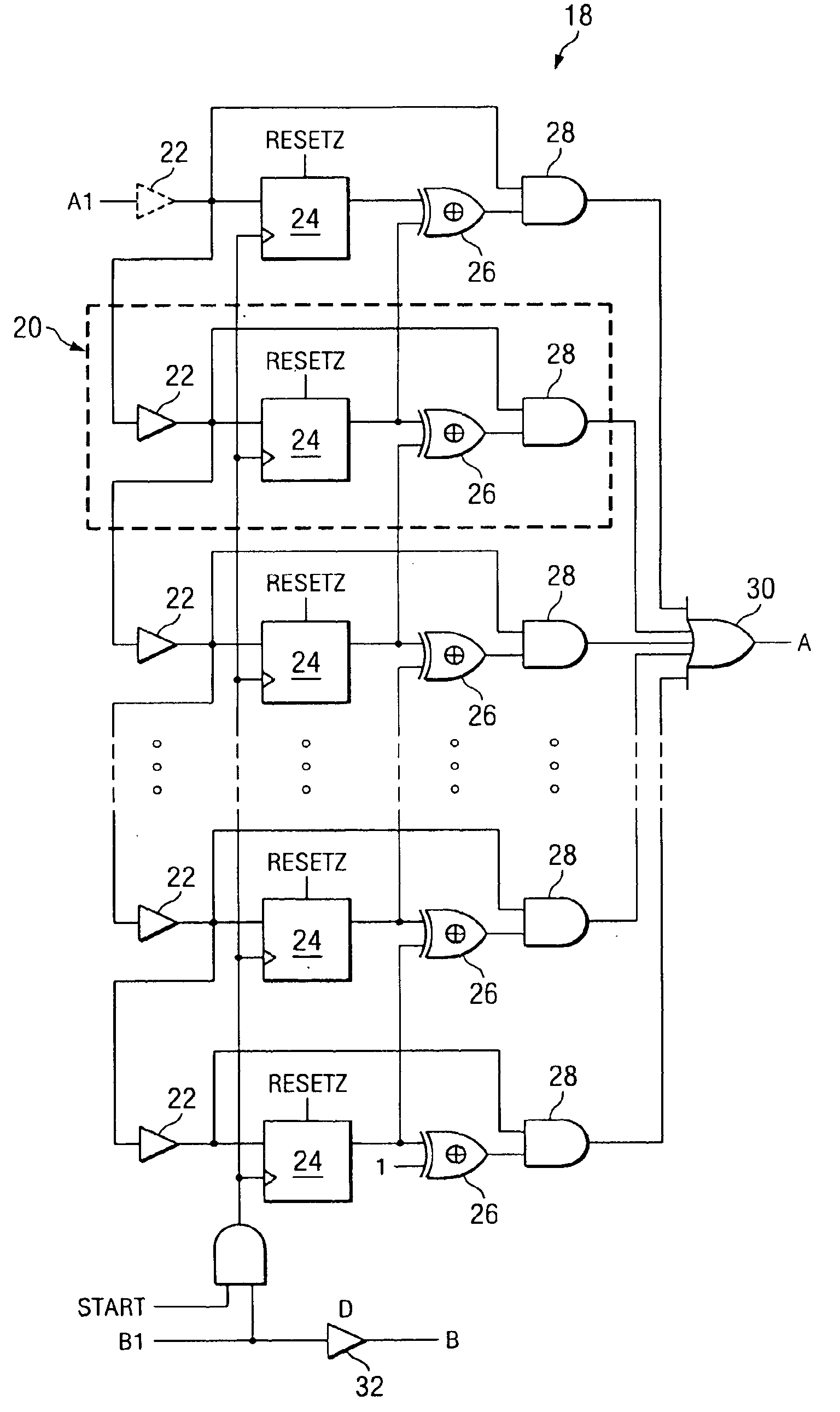
[0021]The present invention is best understood in relation to FIGS. 1-4 of the drawings, like numerals being used for like elements of the various drawings.

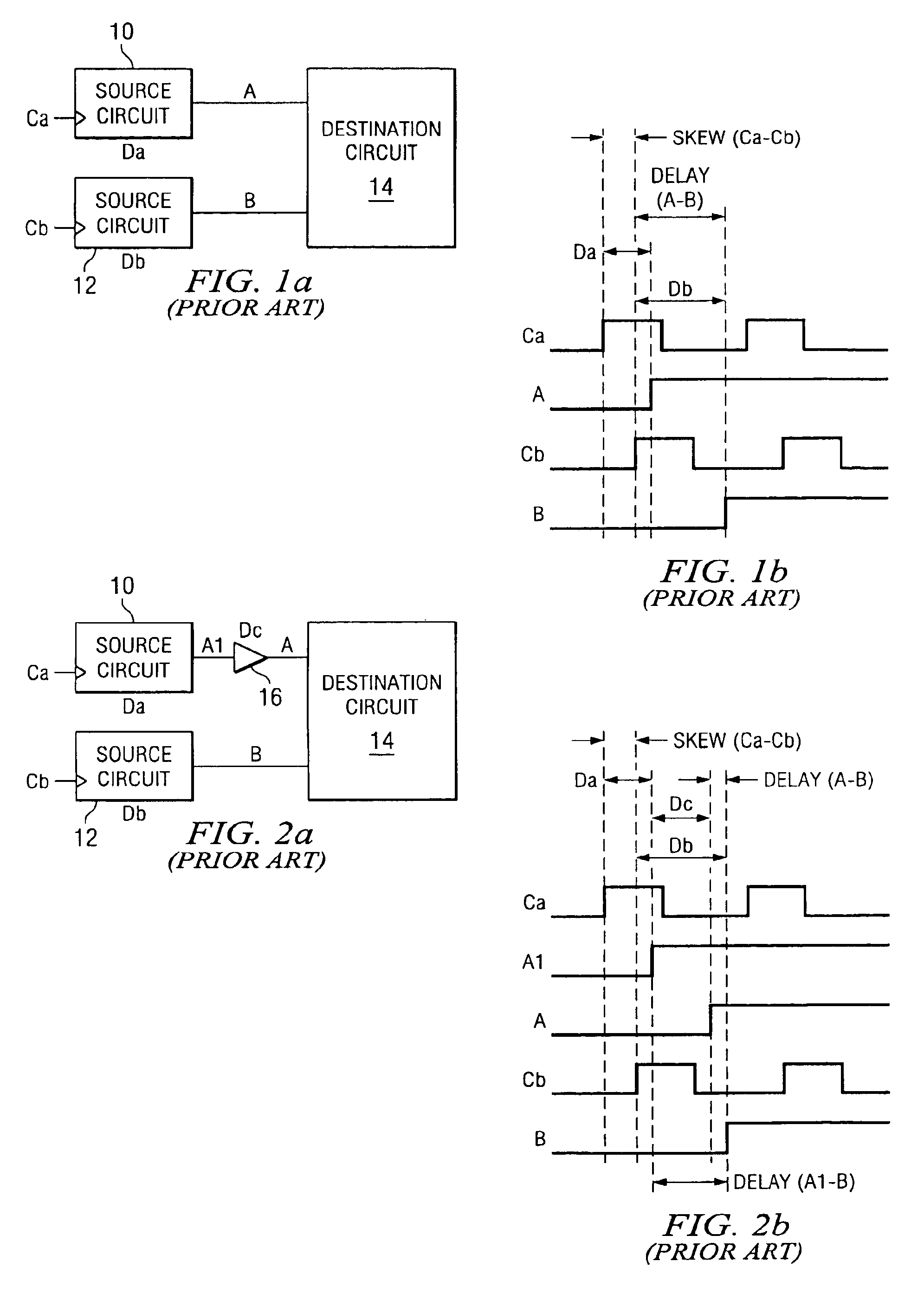
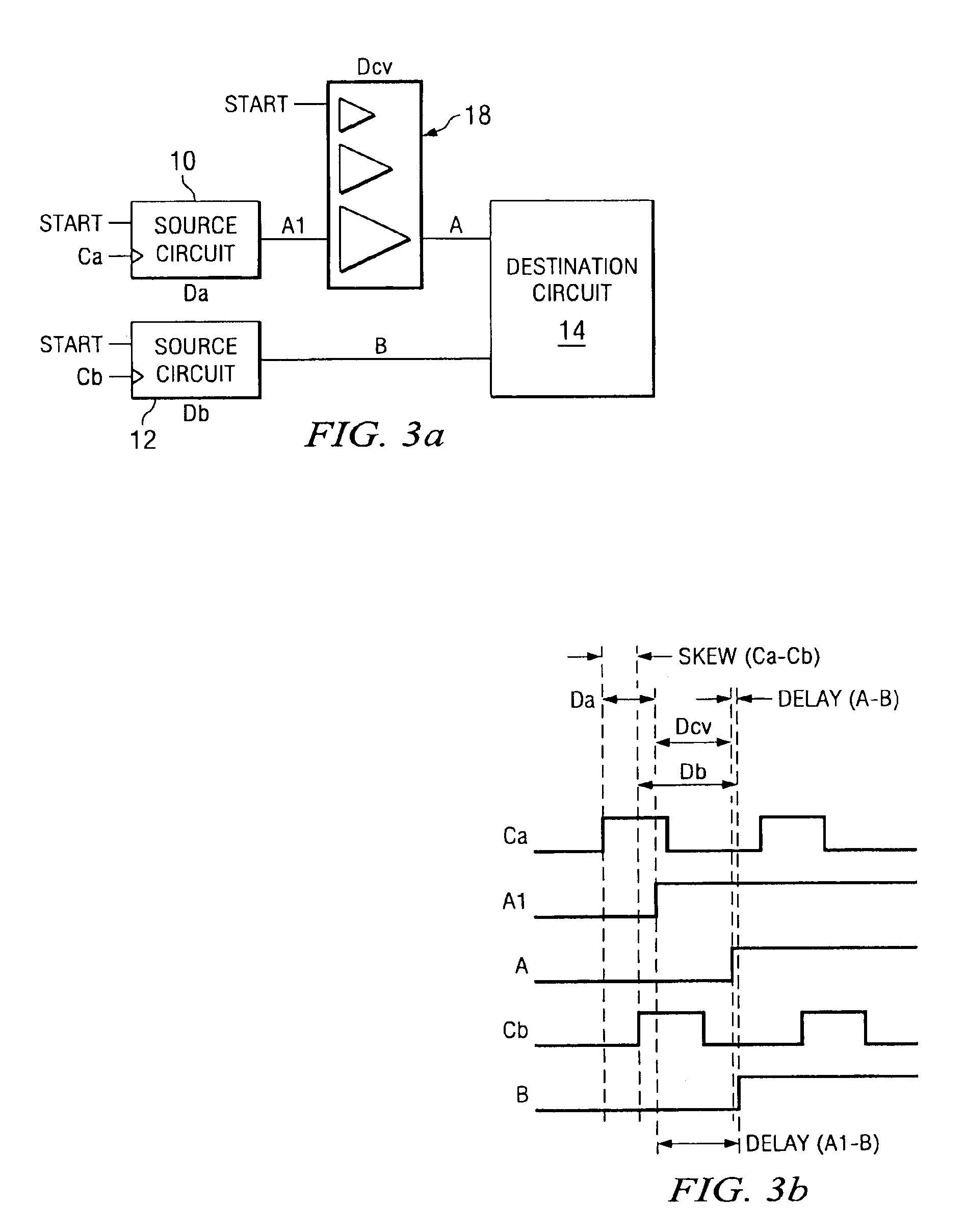
[0022]FIGS. 2a and 2b illustrate a prior art solution to the problem of signal skew. FIG. 2a is the same as the example circuit of FIG. 1a, with the addition of a delay buffer 16 between the output (A1) of source circuitry 10 and the input (A) to user circuitry 14. The delay Dc is calculated to compensate for the delays caused by clock skew and logic and routing delays. With the addition of delay buffer 16, the delay between signals A and B could be estimated as:

Delay(A−B)=Skew(Ca−Cb)+Db−(Da+Dc)

[0023]However, it should be noted that clock and signal delays are not exact, since each has a spread which may very based on processing variations and environmental factors. Some environmental factors, such as temperature, may vary during operation of a device. Hence Ca=Canom±ΔCa, Cb=Cbnom±ΔCb, Da=Danom±ΔDa, Db=Dbnom±ΔDb, and Dc=Dcnom±ΔD...


PUM


Abstract

An electronic integrated circuit includes a first signal (A1) generated by a first source block (10) and a second signal (B1) generated by a second source block (12). A variable delay circuit (18) detects a delay between said first and second signals in calibration mode and applies the delay to the first signal during normal operation of the circuit. A fixed delay buffer (32) may be used to apply a delay to the second signal to compensate for known delays associated with the variable delay circuit (18).

Description

[0001]This application claims priority under 35 USC § 119(e)(1) of European Patent Application Number 03290003.7 filed Jan. 2, 2003.CROSS REFERENCE TO RELATED APPLICATIONS[0002]Not ApplicableSTATEMENT OF FEDERALLY SPONSORED RESEARCH OR DEVELOPMENT[0003]Not ApplicableBACKGROUND OF THE INVENTION[0004]1. Technical Field[0005]This invention relates in general to electronic circuits and, more particularly, to circuitry for reducing the skew between two signals.[0006]2. Description of the Related Art[0007]In the design of electronic circuits, it is often necessary to compensate for skew between two signals arriving at a common block. Traditionally, the skew between the two signals is reduced with the addition of buffers to equalize the difference between the paths of the two signals. Often, the appropriate buffers can be determined automatically using computer aided design tools.[0008]An example of the problem is set forth in connection with FIGS. 1a and 1b. FIG. 1a illustrates an example...

Claims


Application Information

Patent Timeline
Patent Type & Authority Patents(United States)
IPC IPC(8): G06F1/10H04L7/10H03K5/135
CPCG06F1/10H04L7/0037H04L7/10H03K5/135
Inventor JIGUET, JEAN-CHRISTOPHECOPPOLA, FRANCESCO
Owner TEXAS INSTR INC
Why Eureka
Try Eureka