System and method for fabricating openings in a semiconductor topography

a semiconductor topography and contact technology, applied in the direction of semiconductor/solid-state device testing/measurement, electrical equipment, basic electric elements, etc., can solve the problems of reducing the overall cost of fabricating a semiconductor device, occurrence of defects, and increasing manufacturing capacity, so as to reduce the amount of manufacturing cost

Inactive Publication Date: 2005-05-17
MONTEREY RES LLC
View PDF6 Cites 25 Cited by
  • Summary
  • Abstract
  • Description
  • Claims
  • Application Information

AI Technical Summary

Benefits of technology

[0016]In general, the system and method described herein provides a means for controlling the formation of various openings. In particular, the system and method provides feed forward control of an opening etch process, which allows processing parameters to be dynamically updated prior to etching one or more semiconductor topographies. Preferably, the system and method updates the processing parameters prior to etching a single wafer, such that variations of dimensional features within semiconductor topographies of the single wafer can be controlled on a wafer-by-wafer basis. In this manner, feed forward control compensates for structural variations, such as variations in the thickness of a layer, to subsequently form openings having profiles and dimensions, which exhibit little to no deviation from a design specification. More specifically, the system and method provides a means for fabricating high aspect ratio openings having substantially perpendicular sidewalls and minimum acceptable critical dimensions. As such, the system and method provides a means for subsequently forming semiconductor devices that exhibit a substantial increase in speed and reliability over conventional devices. In addition, the system and method provides a means for reducing the number of processing steps and / or the amount of processing time over conventional methods. In this manner, the system and method decreases the occurrence of defects, increases manufacturing capacity, and decreases the overall cost of fabricating a semiconductor device.
[0020]Subsequent to the step of etching, the method may further include measuring a bottom lateral width of the one or more openings formed in the semiconductor topography for the purposes of obtaining post-etch values. In addition, or alternatively, the method may include measuring a post-etch thickness of the etched layer and / or measuring a post-etch top lateral width of the one or more openings. Furthermore, the method may include de ter mining a statistical result of the post-etch values, and comparing such a result to the statistical result of the pre-etch values. In this manner, the step of comparing gradually reduces the variation between the desired results and the processing results, thereby incrementally refining the amount by which the processing parameters are adjusted prior to etching a subsequent semiconductor topography. As such, the method advantageously reduces the amount by which dimensions of subsequently formed openings vary from desired dimensions.

Problems solved by technology

In this manner, the system and method decreases the occurrence of defects, increases manufacturing capacity, and decreases the overall cost of fabricating a semiconductor device.

Method used


Image

  • System and method for fabricating openings in a semiconductor topography
  • System and method for fabricating openings in a semiconductor topography
  • System and method for fabricating openings in a semiconductor topography

Examples


Embodiment Construction

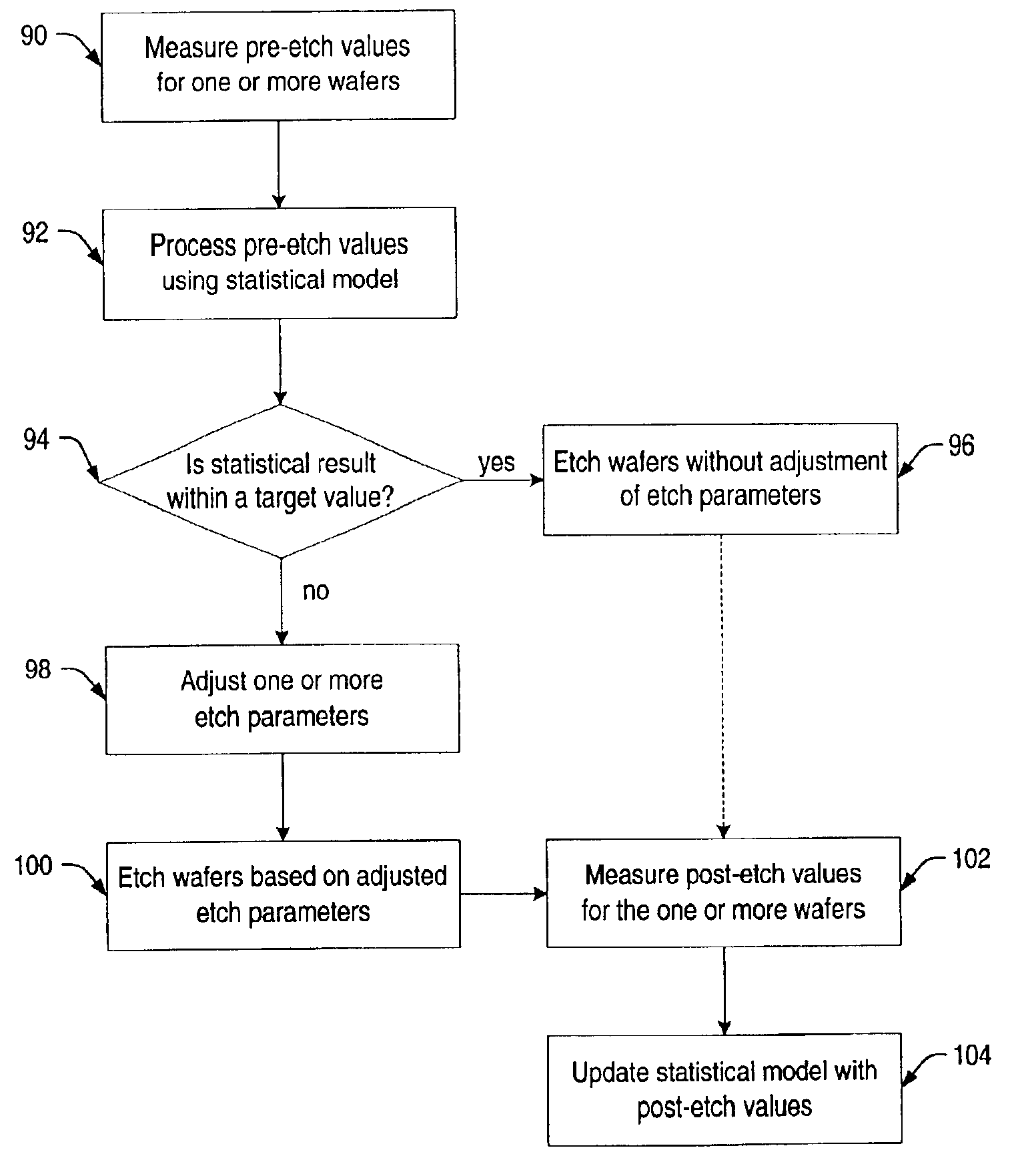
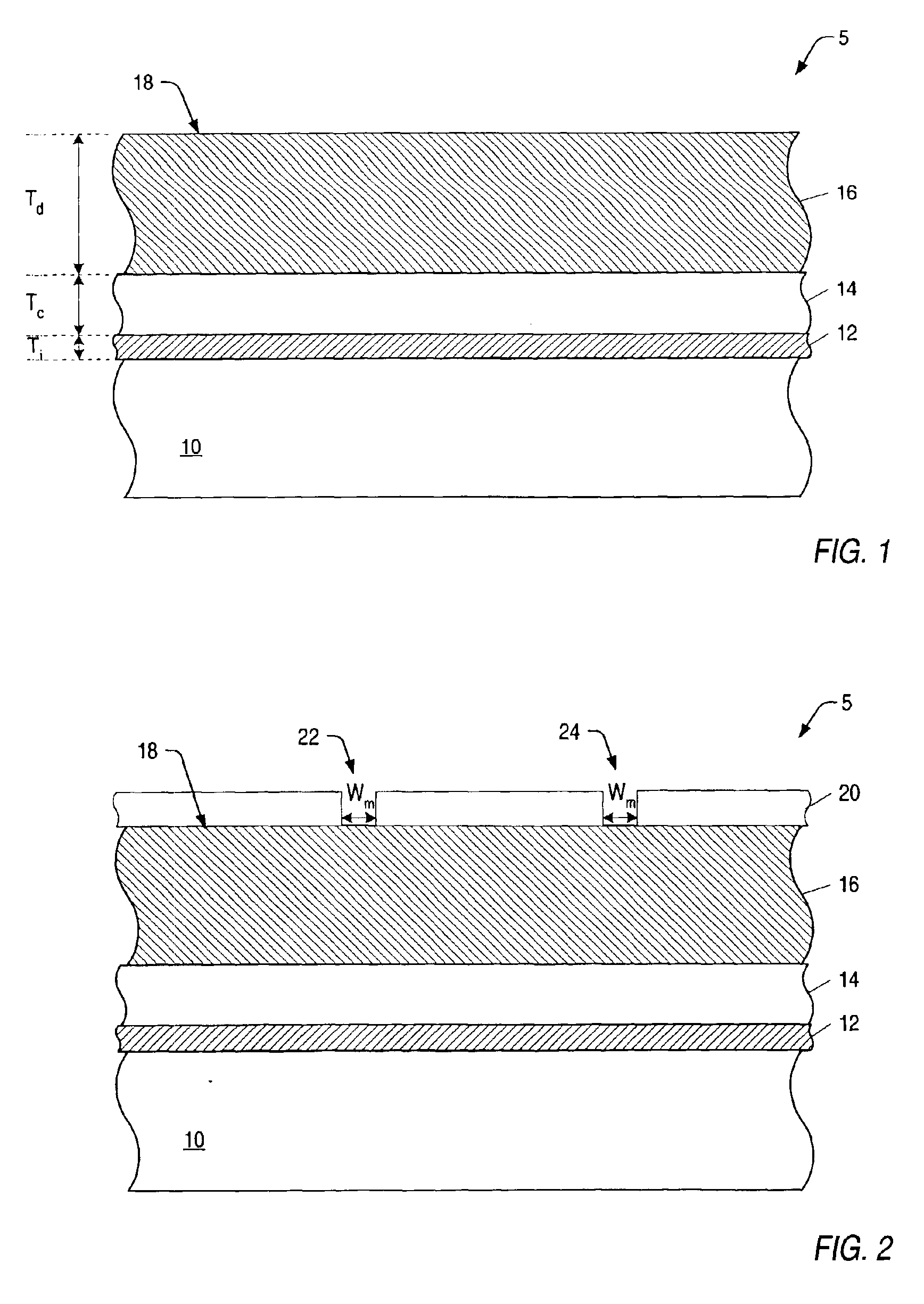
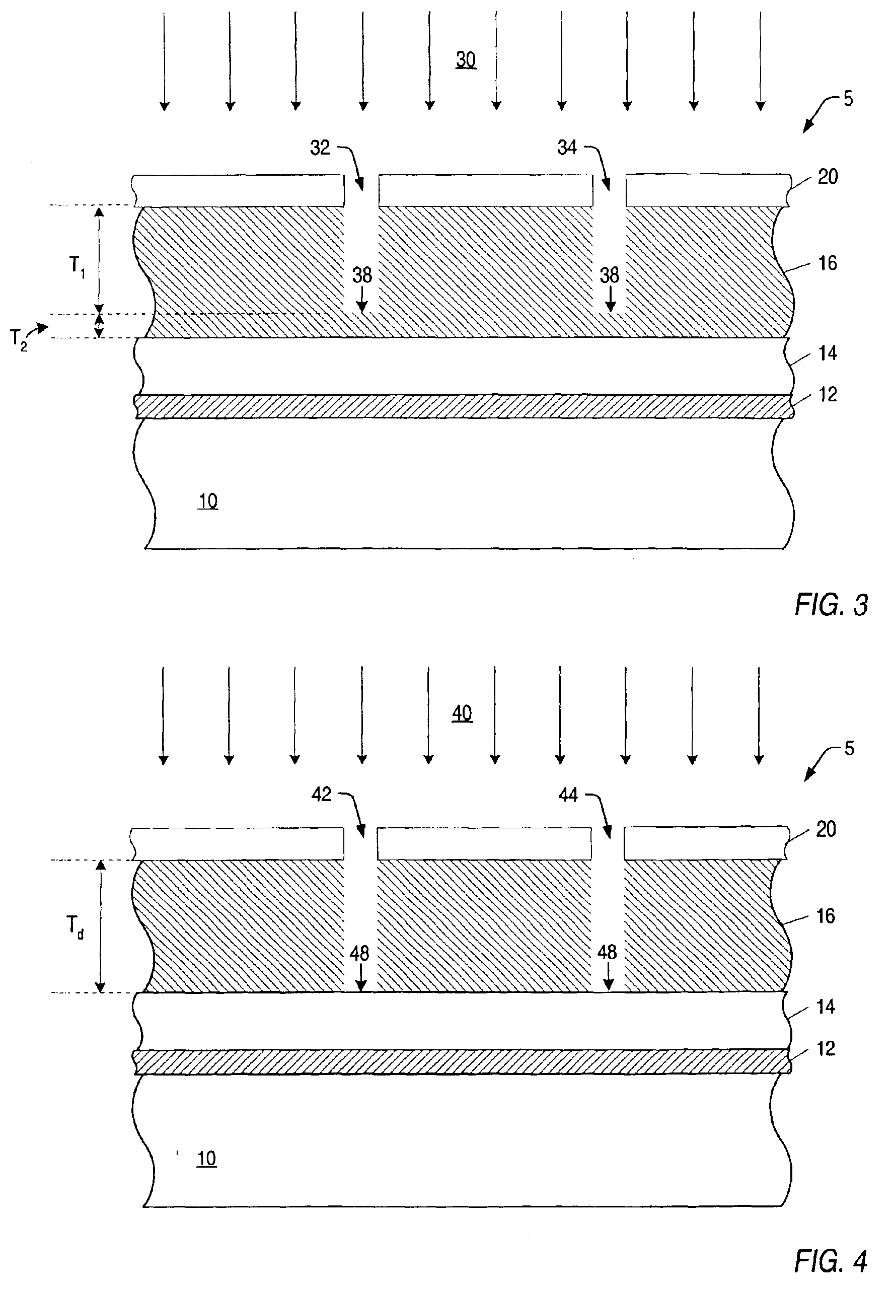
[0040]There are several disadvantages to forming openings (such as, e.g., contact openings and vias) using a conventional single etch processes. For example, a conventional single etch process may use a selective etch chemistry that undesirably deposits a passivating material on the sidewall surfaces of the etched openings. In some cases, the passivating material may cause the amount of tapering in the sidewall surfaces of the etched, openings to steadily increase as the etch process continues. In this manner, the openings may be formed having bottom lateral widths that fall below an acceptable critical dimension, thereby interfacing with the operating characteristics of a subsequently formed contact structure.

[0041]Therefore, in some, embodiments, it may be desirable to form one or more openings using an etch process, which minimizes the use of a selective etch chemistry. Such an etch process may advantageously reduce the amount of tapering produced in the sidewall surfaces of the ...


PUM

PropertyMeasurementUnit
Timeaaaaaaaaaa
Thicknessaaaaaaaaaa
Ratioaaaaaaaaaa

Abstract

A system and method is provided herein to fabricate openings in a semiconductor topography using feed forward control of etch process parameters. In one embodiment, a method includes measuring one or more dimensional features of a semiconductor topography to obtain pre-etch values. The method also includes determining a statistical result of the pre-etch values and adjusting one or more processing parameters if the statistical result is less than a target value. Subsequently, the method includes etching the semiconductor topography based upon the statistical result to form one or more openings in the semiconductor topography. As such, the system and method described herein fabricates openings using feed forward control of the etch process parameters to compensate for structural variations within semiconductor topographies that may exist between wafer-to-wafer and / or between lot-to-lot. In this manner, the system and method advantageously fabricates openings having profiles and dimensions, which exhibit little to no deviation from a design specification.

Description

BACKGROUND OF THE INVENTION[0001]1. Field of the Invention[0002]This invention relates to semiconductor device manufacturing and, more particularly, to an improved system and method for fabricating contact openings in a semiconductor topography.[0003]2. Description of the Related Art[0004]The following descriptions and examples are given as background only.[0005]At various stages in the fabrication of semiconductor devices, it is often necessary to form openings in an inter-level dielectric layer to allow for contact to underlying regions or layers. Generally, an opening through a dielectric layer that exposes a diffusion region, or an opening through a dielectric layer between polysilicon and a first metal layer is called a “contact opening” or a “contact hole.” Conversely, an opening through other dielectric layers such as an opening through an inter-metal dielectric layer is generally referred to as a “via.” For purposes of this disclosure, however, the term “opening” may be used...

Claims


Application Information

Patent Timeline
IPC IPC(8): H01L21/02H01L21/302H01L21/311H01L21/66
CPCH01L21/31116H01L22/20
Inventor SEDIGH, MEHRANCHOWDHURY, SAURABU DUTTA
Owner MONTEREY RES LLC
Why Eureka
Try Eureka