Blue organic electroluminescent devices having a non-hole-blocking layer
a blue el, non-hole blocking technology, applied in the direction of discharge tube luminescnet screens, natural mineral layered products, other domestic articles, etc., can solve the problems of low luminous efficiency, shorten the operational life, and difficulty in achieving high luminous efficiency and good operational life of blue oled, so as to improve the performance of blue oled
- Summary
- Abstract
- Description
- Claims
- Application Information
AI Technical Summary
Benefits of technology
Problems solved by technology
Method used
Image

Examples
example 1
Conventional OLED—Comparative
[0108]The preparation of a conventional blue OLED is as follows: A ˜1.1 mm thick glass substrate coated with a transparent ITO conductive layer was cleaned and dried using a commercial glass scrubber tool. The thickness of ITO is about 42 nm and the sheet resistance of the ITO is about 68 Ω / square. The ITO surface was subsequently treated with oxidative plasma to condition the surface as an anode. A layer of CFx, 1 mm thick, was deposited on the clean ITO surface as the HIL by decomposing CHF3 gas in an RF plasma treatment chamber. The substrate was then transferred into a vacuum deposition chamber (TROVATO MFG. INC) for deposition of all other layers on top of the substrate. The following layers were deposited in the following sequence by evaporation from a heated boat under a vacuum of approximately 10−6 Torr:[0109](1) a HTL, 90 nm thick, consisting of NPB;[0110](2) a LEL, 20 nm thick, consisting of TBADN host material doped with 1.5 vol. % TBP;[0111](...
example 2
Comparative Example
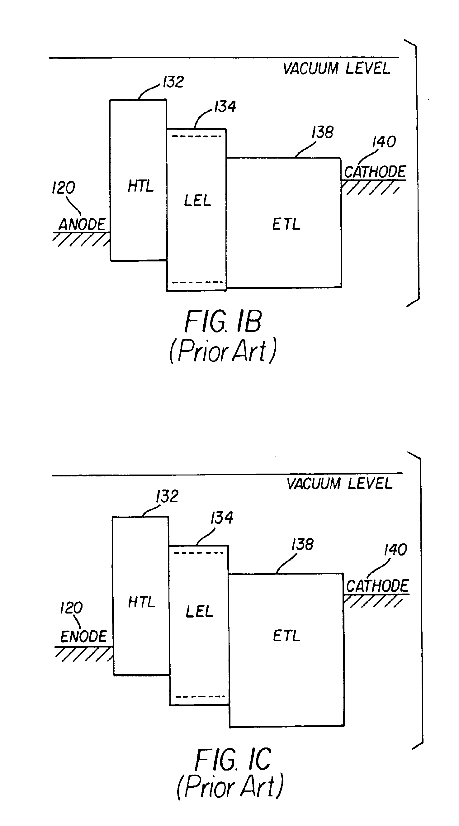
[0115]A blue OLED was constructed in the manner described in Example 1, except in Step 3, the 35 nm Alq ETL is replaced by a 35 nm Bphen ETL. Since Ip(TBADN)=5.8 eV, Eg(TBP)>3.0 eV, Ip(Bphen)=6.5 eV, and Eg(Bphen)=3.4 eV, this device structure has the same electron energy diagram as that shown in FIG. 1C.
[0116]When measured at a current density of 20 mA / cm2, the device has a drive voltage of 7.2 V, luminance of 667 cd / m2, luminous efficiency of 3.34 cd / A, CIEx,y of 0.137, 0.192, and radiance of 3.84 W / Sr / m2. Although the luminous efficiency, radiance, and the color purity of this device are much better than those of Example 1, the operational lifetime of the device is very short because its T80(70° C.)) is less than 30 min. The normalized luminance vs. operational time is shown in FIG. 4.
example 3
Comparative Example
[0117]A blue OLED was constructed in the manner described in Example 1, except in Step 3, the 35 nm Alq ETL is replaced by a 35 nm TPBI ETL. Since Ip(TBADN)=5.8 eV, Eg(TBP)>3.0 eV, Ip(TPBI)=6.2 eV, and Eg(TPBI)=3.4 eV, this device structure has the same electron energy diagram as that shown in FIG. 1C.
[0118]When measured at a current density of 20 mA / cm2, the device has a drive voltage of 7.4 V, luminance of 622 cd / M2, luminous efficiency of 3.11 cd / A, CIEx,y of 0.139, 0.210, and radiance of 3.35 W / Sr / m2. Although the luminous efficiency, radiance, and the color purity of this device are better than those of Example 1, the operational lifetime of the device is short because its T80(70° C.)) is about 8 hours The normalized luminance vs. operational time is shown in FIG. 4.
PUM
| Property | Measurement | Unit |
|---|---|---|
| electron energy band gap | aaaaa | aaaaa |
| emission wavelength | aaaaa | aaaaa |
| thickness | aaaaa | aaaaa |
Abstract
Description
Claims
Application Information
 - R&D
- Intellectual Property
- Life Sciences
- Materials
- Tech Scout
- Unparalleled Data Quality
- Higher Quality Content
- 60% Fewer Hallucinations
Browse by: Latest US Patents, China's latest patents, Technical Efficacy Thesaurus, Application Domain, Technology Topic, Popular Technical Reports.
© 2025 PatSnap. All rights reserved.Legal|Privacy policy|Modern Slavery Act Transparency Statement|Sitemap|About US| Contact US: help@patsnap.com